Color photovoltaic module with improved efficiency and preparation method thereof
A color photovoltaic and solar photovoltaic technology, which is applied in the field of photovoltaic components, can solve the problems of reducing the energy efficiency of photovoltaic chips and solar photovoltaic components, and achieve the effects of reducing shading effects, increasing stereoscopic effects, and reducing production costs
- Summary
- Abstract
- Description
- Claims
- Application Information
AI Technical Summary
Problems solved by technology
Method used
Image
Examples
preparation example Construction
[0035] The second aspect of the present invention provides a method for preparing a color photovoltaic module with improved efficiency, at least including the step of: combining the pattern part with the solar photovoltaic module.
[0036] As a preferred technical solution, the specific printing methods of the white ink layer and the color ink layer in the pattern portion are:
[0037] A: Process the picture with the required pattern through the picture processing software, adjust the picture to grayscale mode, and establish a white spot color channel, and store it as a document 1 that can be recognized by the printing software;
[0038] B: Process the picture with the desired pattern through the picture processing software, set up a curve adjustment layer on the picture, and reduce the blackness value to a minimum, and store it as a document 2 that can be recognized by the printing software;
[0039] C: Edit document one into document three recognizable by the printing softwa...
Embodiment 1
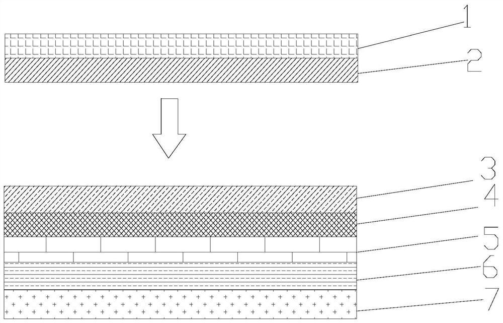
[0046] In order to solve the above technical problems, the first aspect of this embodiment provides a color photovoltaic module with improved efficiency, such as figure 1 Shown includes a white ink layer 2 printed on the solar photovoltaic module, a color ink layer 1 printed on the white ink layer 2, and the solar photovoltaic module includes a first glass layer 3, a first adhesive film layer 4, Photovoltaic chip layer 5 , second adhesive film layer 6 and functional backplane layer 7 , the white ink layer 2 is directly printed on the first glass layer 3 . In this embodiment, the white ink layer 2 and the color ink layer 1 are directly printed on the solar photovoltaic module.
[0047] The thickness of the color ink layer 1 is 0-0.0118mm, and the thickness of the white ink layer 2 is 0-0.02mm.
[0048] The second aspect of this embodiment provides a method for preparing a color photovoltaic module with improved efficiency, including the following steps:
[0049] (1) printing ...
Embodiment 2
[0057] In order to solve the above technical problems, the first aspect of this embodiment provides a color photovoltaic module with improved efficiency, such as figure 2 Shown includes a pattern part and a solar photovoltaic module, the pattern part includes a first glass layer 3, a color ink layer 1 printed on the first glass layer 3, a white ink layer 2 printed on the color ink layer 1, and the solar photovoltaic module The photovoltaic module includes a photovoltaic wafer layer 5 , a second adhesive film layer 6 and a functional backsheet layer 7 from top to bottom, and the white ink layer 2 is bonded to the photovoltaic wafer layer 5 through the first adhesive film layer 4 . In this embodiment, the color ink layer 1 and the white ink layer 2 are printed on the first glass layer 3, and then packaged on the solar photovoltaic module.
[0058] The thickness of the color ink layer 1 is 0-0.0118mm, and the thickness of the white ink layer 2 is 0-0.02mm.
[0059] The second a...
PUM
| Property | Measurement | Unit |
|---|---|---|
| thickness | aaaaa | aaaaa |
| thickness | aaaaa | aaaaa |
| thickness | aaaaa | aaaaa |
Abstract
Description
Claims
Application Information
 - R&D
- Intellectual Property
- Life Sciences
- Materials
- Tech Scout
- Unparalleled Data Quality
- Higher Quality Content
- 60% Fewer Hallucinations
Browse by: Latest US Patents, China's latest patents, Technical Efficacy Thesaurus, Application Domain, Technology Topic, Popular Technical Reports.
© 2025 PatSnap. All rights reserved.Legal|Privacy policy|Modern Slavery Act Transparency Statement|Sitemap|About US| Contact US: help@patsnap.com


