Method for preparing layered bismuth-oxygen-selenium semiconductor film by reverse airflow method
A semiconductor, bismuth oxide technology, applied in chemical instruments and methods, crystal growth, from condensed steam, etc., can solve the problems of uneven nucleation probability of thin layers, and achieve the reduction of uneven nucleation probability, large area and high quality high effect
- Summary
- Abstract
- Description
- Claims
- Application Information
AI Technical Summary
Problems solved by technology
Method used
Image
Examples
Embodiment 1
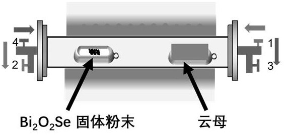
[0046] Such as figure 1 As shown, open the first valve 1, the second valve 2, close the third valve 3, and the fourth valve 4. At this time, the air flow flows from the substrate to the growth raw material, which is a reverse air flow; close the first valve 1, the second valve 2, Open the third valve 3 and the fourth valve 4, and at this time, the airflow flows from the growth raw material to the substrate, which is a positive airflow.
[0047] This embodiment provides a method for preparing a layered bismuth oxide selenide semiconductor thin film by a reverse air flow method, which includes the following steps:
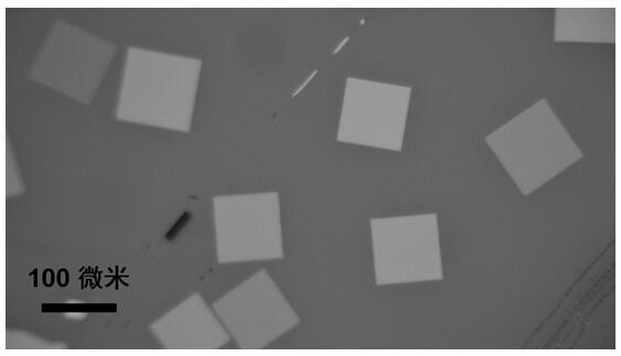
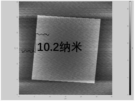
[0048] Weigh Bi 2 o 2 1g of Se powder raw material is placed in the center of the quartz tube furnace. Take the mica substrate and place it at the hearth mouth of the quartz tube furnace (i.e. Bi 2 o 2 6 cm downstream of the Se powder feedstock). Pass the carrier gas argon, the airflow is 200 cubic centimeters per minute, and the airflow direction is reverse ai...
Embodiment 2
[0056] This embodiment provides a method for preparing a layered bismuth oxide selenide semiconductor thin film by a reverse air flow method, which includes the following steps:
[0057] Weigh Bi 2 o 2 1g of Se powder raw material is placed in the center of the quartz tube furnace. Take the mica substrate and place it at the hearth mouth of the quartz tube furnace (i.e. Bi 2 o 2 18 cm downstream of the Se powder raw material). Pass the carrier gas argon, the airflow is 100 cubic centimeters per minute, and the airflow direction is reverse airflow at this time, and the tube furnace is heated at the same time, from room temperature to 700 ° C, and kept at 700 ° C for 30 minutes, After the heat preservation is over, adjust the airflow to a positive airflow and deposit for 12 minutes. After the deposition, the temperature is naturally cooled to room temperature to obtain a layered Bi 2 o 2 Se film.
[0058] The pressure of the whole preparation process is normal pressure. ...
Embodiment 3
[0061] This embodiment provides a method for preparing a layered bismuth oxide selenide semiconductor thin film by a reverse air flow method, which includes the following steps:
[0062] Weigh Bi 2 o 2 2g of Se powder raw material is placed in the center of the quartz tube furnace. Take the mica substrate and place it at the hearth mouth of the quartz tube furnace (i.e. Bi 2 o 2 12 cm downstream of the Se powder raw material). Pass the carrier gas argon, the airflow is 175 cubic centimeters per minute, and the airflow direction is reverse airflow at this time, and the tube furnace is heated at the same time, from room temperature to 720 ° C, and kept at 720 ° C for 20 minutes, After the heat preservation is over, adjust the airflow to a positive airflow and deposit for 6 minutes. After the deposition, the temperature is naturally cooled to room temperature to obtain a layered Bi 2 o 2 Se film.
[0063] The pressure of the whole preparation process is normal pressure.
...
PUM
| Property | Measurement | Unit |
|---|---|---|
| size | aaaaa | aaaaa |
| thickness | aaaaa | aaaaa |
| size | aaaaa | aaaaa |
Abstract
Description
Claims
Application Information
 - R&D Engineer
- R&D Manager
- IP Professional
- Industry Leading Data Capabilities
- Powerful AI technology
- Patent DNA Extraction
Browse by: Latest US Patents, China's latest patents, Technical Efficacy Thesaurus, Application Domain, Technology Topic, Popular Technical Reports.
© 2024 PatSnap. All rights reserved.Legal|Privacy policy|Modern Slavery Act Transparency Statement|Sitemap|About US| Contact US: help@patsnap.com


