
Semi-flexible component carrier and manufacturing method thereof

A component-carrying, semi-flexible technology, applied in semiconductor/solid-state device manufacturing, semiconductor/solid-state device components, circuit bendable/stretchable components, etc., can solve problems such as easy damage, to overcome significant defects, The effect of reducing the bend radius

Active Publication Date: 2021-02-09
AT & S AUSTRIA TECH & SYSTTECHN AG
View PDF12 Cites 1 Cited by
  • Summary
  • Abstract
  • Description
  • Claims
  • Application Information

AI Technical Summary

Problems solved by technology

However, conventional semi-flexible component carriers are prone to damage when bending the semi-flexible portion of the conventional semi-flexible component carrier

Method used


Image

  • Semi-flexible component carrier and manufacturing method thereof
  • Semi-flexible component carrier and manufacturing method thereof
  • Semi-flexible component carrier and manufacturing method thereof

Examples


Embodiment approach

[0064]According to an exemplary embodiment of the present invention, a dielectric low modulus and high elongation material can be applied to a semi-flexible part of a semi-flexible component carrier (especially a printed circuit board, PCB). This can allow small bending radii to be resolved and dynamic bending angles can be achieved on semi-flexible component carriers. In particular, this can be achieved by arranging a dielectric material in at least the semi-flexible part so as to have a low Young's modulus lower than 5 GPa and a high elongation higher than 3%. Therefore, the dielectric material in the semi-flexible portion can be elastic and malleable.

[0065]According to an exemplary embodiment of the present invention, a semi-flexible PCB is provided with a semi-flexible portion of a dielectric material, which has a low Young's modulus lower than 5 GPa and a high elongation higher than 3%. Traditionally, PCBs are only used for high bend radius applications with estimated radii gre...


PUM

PropertyMeasurementUnit
elongationaaaaaaaaaa
lengthaaaaaaaaaa
elongationaaaaaaaaaa

Abstract

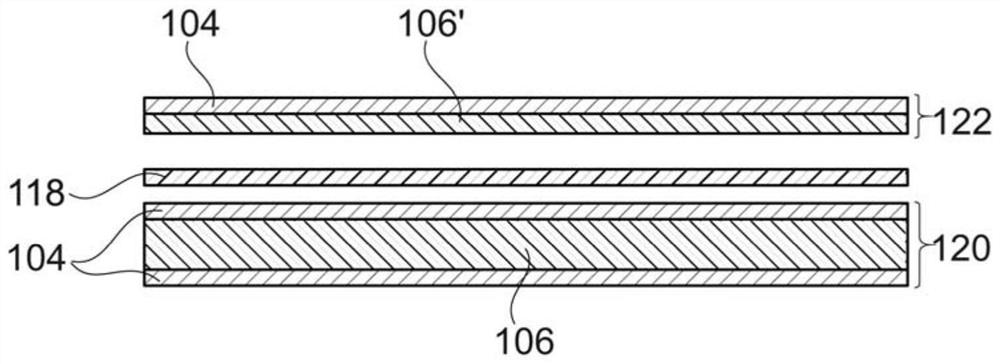
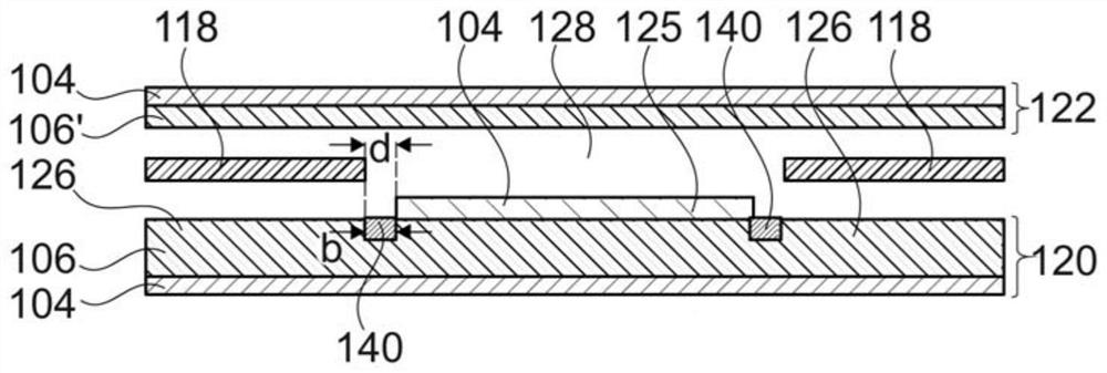
The invention discloses a semi-flexible component carrier (100). The semi-flexible component carrier comprises stack (102) comprising at least one electrically insulating layer structure (106) and / orat least one electrically conductive layer structure (104), wherein the stack (102) defines at least one rigid portion (108) and at least one semi-flexible portion (110); at least one electrically insulating layer structure (106') of the at least one electrically insulating layer structure (106) forming at least a portion of the semi-flexible portion (110) comprises a material having an elongationgreater than 3% and a Young's modulus less than 5 GPa. The invention also relates to a manufacturing method of the semi-flexible component carrier.

Description

Technical field[0001]The invention relates to a semi-flexible component carrier and to a method of manufacturing a semi-flexible component carrier.Background technique[0002]Product functions in component carriers equipped with one or more electronic components are increasing, and the miniaturization of such components continues to increase, and the number of components to be mounted on component carriers such as printed circuit boards In the context of increasing numbers, more and more powerful array-like components or packages with several components are used, which have multiple contacts or connections, and the spacing between these contacts or connections is getting smaller and smaller. Removal of the heat generated by these components and the component carrier itself during operation has become an increasingly serious problem. At the same time, the component carrier should be mechanically strong and electrically reliable in order to be operable even under severe conditions.[0003...

Claims


Application Information

Patent Timeline
Patent Type & Authority Applications(China)
IPC IPC(8): H01L23/498H01L23/14H01L21/48
CPCH01L23/49822H01L23/498H01L23/145H01L21/4846H01L21/4857H05K1/185H05K3/4691H05K2201/09127H05K2201/0133H05K1/0278H05K1/189H05K3/4655H05K1/183
Inventor 辛利宁米凯尔·图奥米宁郑惜金
Owner AT & S AUSTRIA TECH & SYSTTECHN AG
Learn More