VCSEL chip gold film etching solution and etching method thereof

An etching solution and chip technology, applied in chemical instruments and methods, surface etching compositions, electrical components, etc., can solve problems such as large roughness and irregular morphology of electroplated gold layer, and achieve improved affinity and high etching. The effect of precision

Active Publication Date: 2021-02-05
威科赛乐微电子股份有限公司
View PDF7 Cites 1 Cited by
  • Summary
  • Abstract
  • Description
  • Claims
  • Application Information

AI Technical Summary

Problems solved by technology

[0005] In view of this, the purpose of the present invention is to provide a kind of VCSEL chip gold film etchant and its etching method, so that the VCSEL chip gold film etching uniform appearance becomes better, and effectively solve the VCSEL chip remaining electroplating by wet process gold film etching. The morphology of the gold layer is seriously irregular and the roughness is large

Method used


Image

  • VCSEL chip gold film etching solution and etching method thereof
  • VCSEL chip gold film etching solution and etching method thereof
  • VCSEL chip gold film etching solution and etching method thereof

Examples


Embodiment Construction

[0024] The present invention will be described in detail below in conjunction with accompanying drawing:

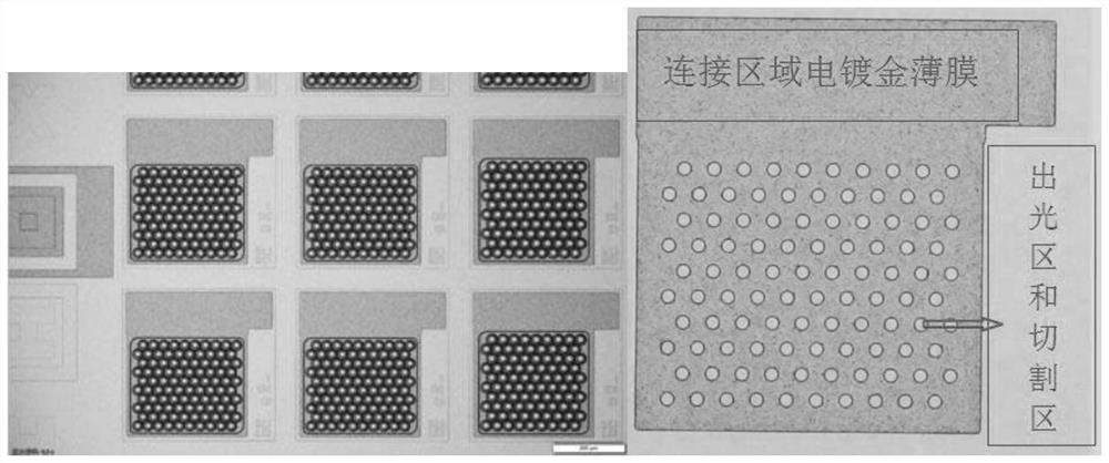
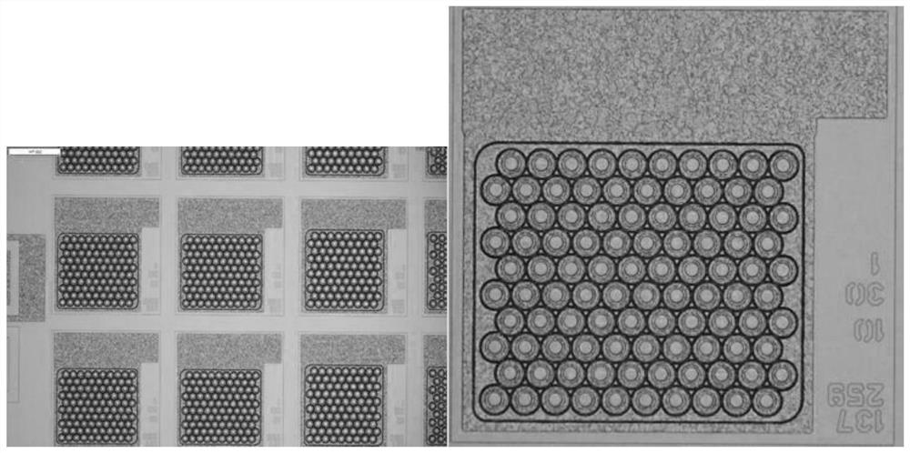
[0025] Taking the wafer after the electroplating process in a certain VCSEL chip manufacturing process as an example, the gold thin film is etched, as shown in figure 1 As shown, there are two gold films with different thicknesses on the surface of the wafer. figure 1 Among them, the area with small black spots is the electrode connection area, and its surface is an electroplated gold film with a thickness of about 3.5um; the rest of the area is the light emitting area and the cutting area, and its surface is a sputtered gold film with a thickness of about 200nm. In the following embodiments, the 200nm gold film will be etched away using an etchant, that is, the gold film in the light emitting area and the cutting area will be completely etched away.

[0026] In the iodine-potassium iodide-water solution in the following examples, every 1L of water contains the iodine of...


PUM


Abstract

The invention relates to the technical field of chip manufacturing, and discloses a VCSEL chip gold film etching solution and an etching method thereof, the etching solution comprises an iodine-potassium iodide-aqueous solution and an alcohol, the etching method of the VCSEL chip gold film uses the etching solution, and the etching method comprises the following steps: adding the alcohol into theiodine-potassium iodide-aqueous solution, stirring uniformly to obtain an etching liquid, then putting the wafer subjected to the electroplating process in the VCSEL chip manufacturing process into anetching solution, standing and soaking, and after sputtered gold is completely etched, washing with water and drying. According to the method, the gold film of the VCSEL chip is etched uniformly, themorphology of the gold film becomes better, and the problems that after the VCSEL chip is etched through the wet gold film, the morphology of a residual electroplated gold layer is irregular, and theroughness is large are effectively solved.

Description

technical field [0001] The invention relates to the technical field of chip manufacturing, in particular to a VCSEL chip gold film etchant and an etching method thereof. Background technique [0002] Because of its high electrical conductivity, high thermal conductivity, good chemical stability and good corrosion resistance, gold is often used as the conductive layer material of thin film devices and semiconductor devices to complete the transmission of electrical signals. The patterning of the conductive gold layer can be realized by etching technology. The etching technology includes wet etching and dry etching. The wet etching is completed in the solution, obeys the isotropic etching mechanism, and has the advantages of fast speed and simple device. and easy operation. [0003] In the production process of VCSEL (Vertical Cavity Surface Emitting Laser) chips, wet etching of gold thin films is a commonly used production process for VCSEL chips. Its role is to transfer the...

Claims


Application Information

Patent Timeline
Patent Type & Authority Applications(China)
IPC IPC(8): C09K13/00H01L21/3213
CPCC09K13/00H01L21/32134
Inventor 李雪松刘春梅
Owner 威科赛乐微电子股份有限公司
Why Eureka
Try Eureka