Array substrate, preparation method thereof and display device
What is Al technical title?
Al technical title is built by PatSnap Al team. It summarizes the technical point description of the patent document.
A technology for array substrates and display areas, applied in semiconductor/solid-state device manufacturing, semiconductor devices, electrical components, etc., can solve the problem of dark lines in the display area, and achieve the effect of avoiding dark lines
Active Publication Date: 2021-01-29
KUNSHAN GO VISIONOX OPTO ELECTRONICS CO LTD
View PDF2 Cites 4 Cited by
Summary
Abstract
Description
Claims
Application Information
AI Technical Summary
This helps you quickly interpret patents by identifying the three key elements:
Problems solved by technology
Method used
Benefits of technology
Problems solved by technology
[0004] The technical problem to be solved by the present invention is to overcome the problem of dark lines in the display area in the prior art
Method used
Image
Click on the blue label to locate the original text in one second.
Reading with bidirectional positioning of images and text.
Examples
Embodiment Construction
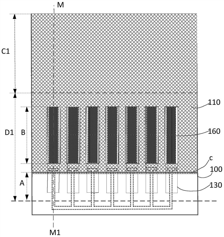
[0035] As mentioned in the background, dark lines are easily generated in the display area of the array substrate in the prior art.
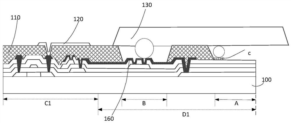
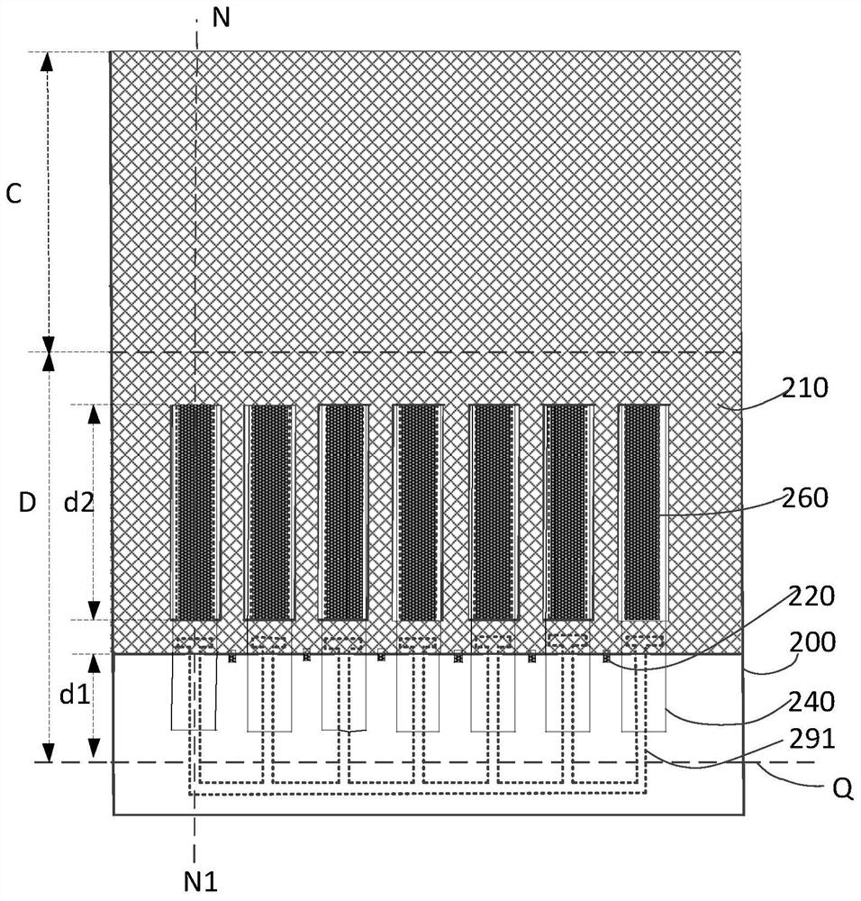
[0036] An array substrate, combined with reference figure 1 with figure 2, including: a base substrate 100, the base substrate 100 includes a display area C1 and an edge area D1, the edge area D1 includes a cutting reserved area A and a binding area B, and the binding area B is located on the display between the area C1 and the reserved area for cutting; the planarization layer 110 located on the display area C1 and the edge area D1, and the planarization layer 110 exposes the reserved area for cutting and the Binding area B; anode layer 120, located on the display area C1 and on the surface of the planarization layer 110 away from the base substrate 100; electrically connected to the conductive connection line 160 of the binding area B There are several bonding connection lines 130 , and the bonding connection lines 130 extend from the bin...
PUM
Abstract
The invention discloses an array substrate, a preparation method thereof and a display device. The array substrate comprises: a substrate, wherein the substrate comprises a display area and an edge area, the edge area comprises a cutting reserved area and a binding area, and the binding area is located between the display area and the cutting reserved area; a planarization layer located on the display area and the edge area, wherein the planarization layer exposes the cutting reserved area and the binding area; an electrode spacer which is positioned on a part of the cutting reserved area andis in contact with the planarization layer; an electrode layer located on the display area and located on the surface of the side, deviating from the underlayer substrate, of the planarization layer;and a plurality of binding connecting wires electrically connected with the binding area, wherein the binding connecting wires extend from the binding area to the cutting reserved area along the top surface of the planarization layer. The electrode spacer is arranged on the cutting reserved area between the adjacent binding connecting wires. According to the array substrate, dark lines in the display area can be avoided.
Description
technical field [0001] The present invention relates to the field of display technology, in particular to an array substrate, a preparation method thereof, and a display device. Background technique [0002] Organic Light-Emitting Diode (OLED) display is a display device with great development prospects. It not only has excellent display performance, but also has self-illumination, simple structure, ultra-thin, fast response, wide Viewing angle, low power consumption, and flexible display can be realized, which are favored by major display manufacturers. Compared with LCD displays, OLED displays are thin, light, wide viewing angle, active luminescence, continuously adjustable luminous color, low cost, fast response, low energy consumption, low driving voltage, wide operating temperature range, simple production process, and luminous It has the advantages of high efficiency and flexible display, and its investment in production equipment is much smaller than that of LCD disp...
Claims
Application Information
Patent Timeline
Application Date:The date an application was filed.
Publication Date:The date a patent or application was officially published.
First Publication Date:The earliest publication date of a patent with the same application number.
Issue Date:Publication date of the patent grant document.
PCT Entry Date:The Entry date of PCT National Phase.
Estimated Expiry Date:The statutory expiry date of a patent right according to the Patent Law, and it is the longest term of protection that the patent right can achieve without the termination of the patent right due to other reasons(Term extension factor has been taken into account ).
Invalid Date:Actual expiry date is based on effective date or publication date of legal transaction data of invalid patent.