A pixel structure and liquid crystal panel

A pixel structure and pixel technology, applied in the direction of instruments, nonlinear optics, optics, etc., can solve the problems affecting the use function of the liquid crystal panel, damaging the pixel penetration rate, increasing the liquid crystal alignment, etc., to improve the display quality, optimize the alignment electric field, The effect of improving the compensation ability

Active Publication Date: 2022-02-22
TCL CHINA STAR OPTOELECTRONICS TECH CO LTD
View PDF0 Cites 0 Cited by
  • Summary
  • Abstract
  • Description
  • Claims
  • Application Information

AI Technical Summary

Problems solved by technology

[0005] The embodiment of the present invention provides a pixel structure and a liquid crystal panel, which can solve the problem that in the prior art, when designing the pixels of the VA liquid crystal panel, the metal traces occupy the pixel space, and the conventional design of the pixel electrode area below the color resistance area is a long and narrow strip. Shape, and the aspect ratio of the pixel electrode area is 3:1, it is easy to produce irregular liquid crystal dark lines, the original cross-shaped dark lines become irregular and distorted multiple dark lines, which increases the risk of abnormal alignment of liquid crystals, which seriously affects The use function of the LCD panel, the technical problem of impairing the pixel transmittance

Method used


Image

  • A pixel structure and liquid crystal panel
  • A pixel structure and liquid crystal panel
  • A pixel structure and liquid crystal panel

Examples


Embodiment Construction

[0032] The following will clearly and completely describe the technical solutions in the embodiments of the present invention with reference to the drawings in the embodiments of the present invention. Apparently, the described embodiments are only some of the embodiments of the present invention, but not all of them. Based on the embodiments of the present invention, all other embodiments obtained by those skilled in the art without creative efforts fall within the protection scope of the present invention.

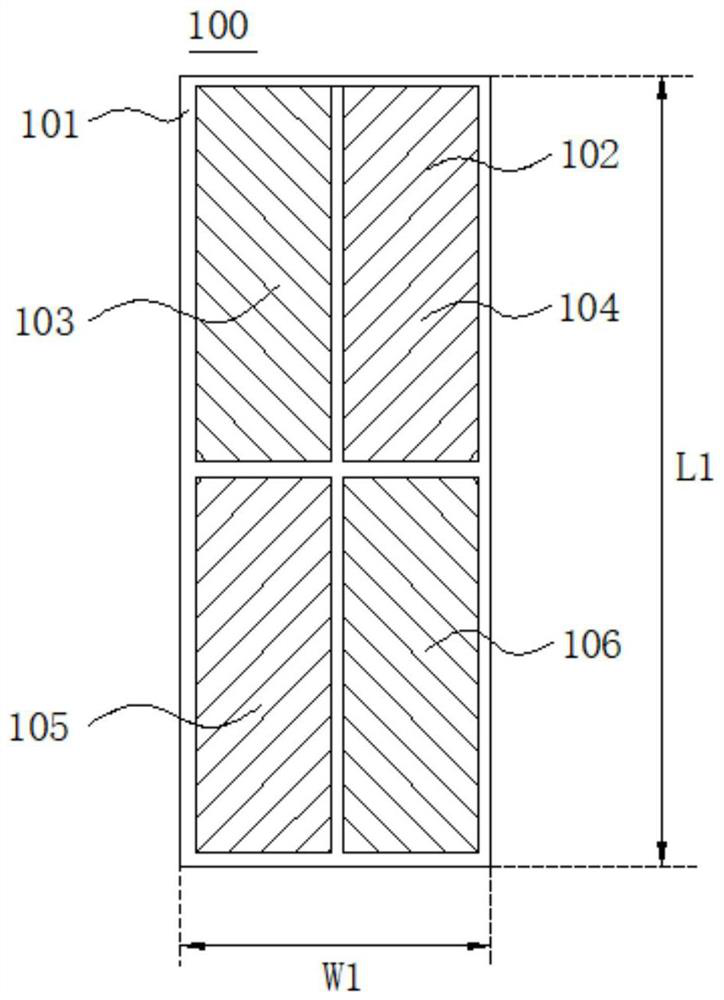
[0033] The present invention aims at designing the pixels of the liquid crystal panel in the prior art, because the metal wires occupy the pixel space, the pixel electrode area is conventionally designed under the color resistance area, which is in the shape of a long and narrow strip, and the aspect ratio of the pixel electrode area is 3:1 , it is easy to produce irregular liquid crystal dark lines, and the original rectangular edge sealing and rice font will become irr...


PUM


Abstract

The present invention provides a pixel structure and a liquid crystal panel. The pixel structure includes a pixel electrode. The pixel electrode includes a trunk electrode, a branch electrode connected to the trunk electrode, and a sealing electrode surrounding the trunk electrode and the branch electrode. The trunk electrode is connected to at least one end of the branch electrode. A sealing electrode; wherein, a gap electrode is formed on the long side of the sealing electrode, and the gap electrode extends into the pixel structure, and the pixel electrode is divided into at least two pixel partitions, so that the original one pixel partition becomes a plurality of pixel partitions, Using the notch to reduce the aspect ratio of the pixel partition, and adding a horizontal trunk electrode in the divided pixel partition, further dividing the divided pixel partition into multiple pixel domains, shortening the length of the branch electrodes and reducing the impedance of the pixel electrodes, The compensation ability of the liquid crystal driving signal is improved, so that the abnormal dark lines of the entire pixel structure are avoided, and the display quality of the pixel structure is improved.

Description

technical field [0001] The invention relates to the field of display technology, in particular to a pixel structure and a liquid crystal panel. Background technique [0002] Usually, the liquid crystal display panel is composed of a color film substrate, a thin film transistor substrate, a liquid crystal sandwiched between the color film substrate and the thin film transistor substrate, and a sealant; its working principle is to control the liquid crystal layer by applying a driving voltage on two glass substrates. The rotation of the liquid crystal molecules refracts the light from the backlight module to produce a picture. The high vertical alignment liquid crystal driving method has the characteristics of high contrast, large aperture ratio and fast deflection speed of liquid crystal molecules. It is one of the key investment areas for TFT-LCD display panel factories in the mainstream market. [0003] HVA technology requires liquid crystal molecules to be negative liquid...

Claims


Application Information

Patent Timeline
Patent Type & Authority Patents(China)
IPC IPC(8): G02F1/1343
CPCG02F1/134309
Inventor 刘毅
Owner TCL CHINA STAR OPTOELECTRONICS TECH CO LTD
Why Eureka
Try Eureka