Selective wave soldering method and system for PCB repair

A PCB board and selective technology, applied in the field of selective wave soldering methods and systems for PCB board repair, can solve the problems of time-consuming, laborious, misjudgment and missed judgment, so as to improve the product qualification rate and avoid misjudgment and leakage. The effect of judgment and time saving

Pending Publication Date: 2021-01-22
ALEADER VISION TECH
View PDF5 Cites 1 Cited by
  • Summary
  • Abstract
  • Description
  • Claims
  • Application Information

AI Technical Summary

Problems solved by technology

Nowadays, after using selective wave soldering to repair PCB boards, it is still necessary to manually judge whether all repairs are successful (because if there are solder joints that cannot be repaired by machines, manual repairs are required), which is not only time-consuming and laborious, but also easily leads to misjudgments and missed judgments.

Method used


Image

  • Selective wave soldering method and system for PCB repair
  • Selective wave soldering method and system for PCB repair

Examples


Embodiment Construction

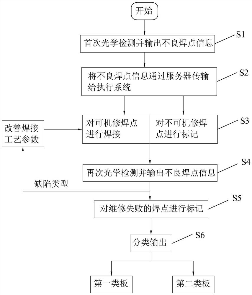
[0042] In order to describe the technical content, structural features, achieved goals and effects of the present invention in detail, the following will be described in detail in conjunction with the embodiments and accompanying drawings.

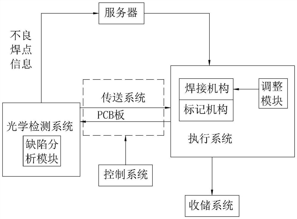
[0043] like figure 1 As shown, this embodiment discloses a selective wave soldering method for repairing a PCB, that is, the defective solder joints on the PCB are repaired through a selective wave soldering process. Specifically, the selective wave soldering method includes the following steps:

[0044]S1: Use the optical inspection system to inspect the solder joints on the PCB board to be processed to obtain information on bad solder joints on the PCB. The bad solder joint information includes the bad type of bad solder joints and the coordinates of the solder joints. The bad types include machine repairable (defective) Relatively light, it can be automatically repaired by machine welding) and not machine repairable (the defect is rela...


PUM


Abstract

The invention discloses a selective wave soldering method and system for PCB repair. The method comprises the following steps: firstly, carrying out the welding spot detection of a to-be-processed PCBthrough an optical detection system, so as to obtain the bad welding spot information of the PCB; then, according to the bad welding spot information, for a welding spot capable of being repaired bya machine, performing welding and maintaining on the welding spot by a welding mechanism according to a welding spot coordinate; for the welding spots which cannot be repaired by the machine, markingthe welding spot by a marking mechanism according to a welding spot to form identification marks; then, detecting the PCB again through an optical detection system, and outputting bad welding spot information again; and finally, marking the welding spots which fail to be maintained through the marking mechanism. According to the selective wave soldering method and system, the PCB is maintained, automatic detection of the selective wave soldering repairing effect is achieved, misjudgment and missed judgment are avoided, the product percent of pass is increased, and the time for searching for welding spots which cannot be repaired by a machine again during manual maintenance can be saved.

Description

technical field [0001] The invention relates to the technical field of selective wave soldering, in particular to a selective wave soldering method and system for PCB board repair. Background technique [0002] Excellent nozzle design in the selective wave soldering process allows soldering parameters to correspond to defined solder joints without subjecting the entire assembly to unnecessary thermal stress, which essentially eliminates the risk of damaging surface mount devices. In view of the precision soldering process of selective wave soldering, generally selective wave soldering is used in the welding of precision instruments and equipment, as well as in the repair of PCBs. [0003] In the use of selective wave soldering for PCB board repair, AOI testing equipment is generally equipped. The AOI testing equipment is used to detect the coordinates of bad solder joints on the PCB. Selectively repair the bad solder joints on the PCB. Nowadays, after using selective wave ...

Claims


Application Information

Patent Timeline
IPC IPC(8): B23K3/00B23K3/08H05K3/34
CPCB23K3/00B23K3/08H05K3/34
Inventor 王锦峰何书德
Owner ALEADER VISION TECH
Why Eureka
Try Eureka