
System-on-chip testing method and system-on-chip

A system-on-a-chip and design scheme technology, applied in computer-aided design, computing, instruments, etc., can solve problems such as large resource consumption, achieve the effect of improving operating speed and reducing verification test costs

Active Publication Date: 2021-04-09
PENG CHENG LAB
View PDF10 Cites 0 Cited by
  • Summary
  • Abstract
  • Description
  • Claims
  • Application Information

AI Technical Summary

Problems solved by technology

[0004] The main purpose of the present invention is to provide a testing method for a SoC chip design scheme and a SoC, aiming to solve the problem of large resource consumption caused by the SoC chip testing process in the prior art

Method used


Image

  • System-on-chip testing method and system-on-chip
  • System-on-chip testing method and system-on-chip
  • System-on-chip testing method and system-on-chip

Examples


Embodiment Construction

[0035] It should be understood that the specific embodiments described here are only used to explain the present invention, not to limit the present invention.

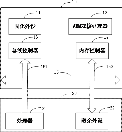
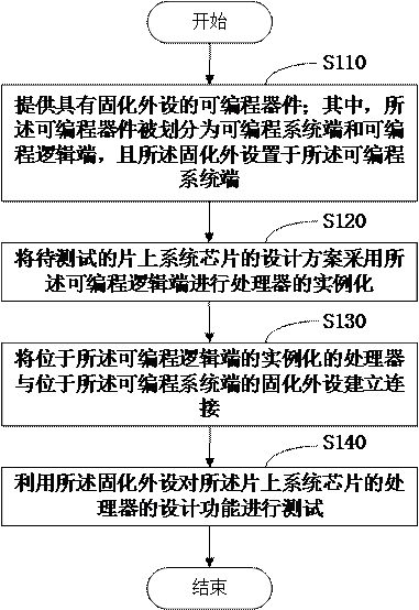
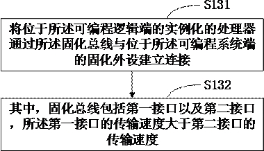
[0036] In order to solve the problem of large resource consumption caused by the system-on-chip chip testing process in the prior art, this application adopts a programmable device with solidified peripherals; wherein, the programmable device is divided into programmable system end and programmable logic end, and the hardened external device is set on the programmable system end; the design scheme of the system-on-chip chip to be tested is instantiated by using the programmable logic end; the instance at the programmable logic end The optimized processor establishes a connection with the solidified peripherals located at the programmable system end; the technical solution of using the solidified peripherals to test the design function of the processor of the SoC reduces the verification of the SoC. cost of testing.

...


PUM


Abstract

The invention discloses a testing method for a system-on-chip chip design scheme, comprising the following steps: providing a programmable device with solidified peripherals; wherein, the programmable device is divided into a programmable system end and a programmable logic end, and The curing device is set on the programmable system end; the design scheme of the system-on-chip chip to be tested is instantiated by the programmable logic end; the instantiated processor located at the programmable logic end Establish a connection with the cured peripherals located at the programmable system end; use the cured peripherals to test the design function of the processor of the SoC chip; the invention also discloses a SoC, which solves The system-on-chip testing process leads to the problem of large resource consumption, which reduces the verification test cost of the system-on-chip.

Description

technical field [0001] The present application relates to the field of FPGA design, in particular to a method for testing a system-on-chip design scheme and a system-on-chip. Background technique [0002] Before the SOC (system on chip) is released, it is necessary to use FPGA (programmable gate array) to test its function and performance, so as to eliminate the functional problems in the system as much as possible, and at the same time ensure that the performance can meet the requirements. Common SOC systems generally It includes one or more processor or controller modules, bus, and multiple peripheral modules that communicate through the bus. Each part of the module will occupy a large amount of FPGA resources. In order to use the most complete system for testing, add as many When the peripheral modules participate in the test, the consumption of FPGA resources will be very large. It is necessary to purchase an FPGA with a larger area for system construction, and the cost ...

Claims


Application Information

Patent Timeline
Patent Type & Authority Patents(China)
IPC IPC(8): G06F30/331
CPCG06F30/331
Inventor 李锐戈黄哲宋雪张凡
Owner PENG CHENG LAB
Learn More