Growth method of miniature light-emitting diode epitaxial wafer

A technology of light-emitting diodes and growth methods, which is applied in the field of growth of micro-light-emitting diode epitaxial wafers, and can solve the problems of increased impurity content, falling, and affecting the crystal quality of epitaxial wafers, etc.

Active Publication Date: 2021-01-01
HC SEMITEK SUZHOU
View PDF10 Cites 0 Cited by
  • Summary
  • Abstract
  • Description
  • Claims
  • Application Information

AI Technical Summary

Problems solved by technology

Wherein, during the growth process of the above-mentioned epitaxial wafer in the reaction chamber, some by-products generated during the growth will be deposited on the side wall of the reaction chamber, so that the impurity content in the reaction chamber will increase, and will eventually fall onto the epitaxial wafer. Particles are generated on the surface, which affects the crystal quality of the epitaxial wafer
Especially for small micro-LEDs, the sum of the volumes of particles falling on the surface of the micro-LEDs may be greater than the volume of the micro-LEDs, resulting in failure of the micro-LEDs

Method used


Image

  • Growth method of miniature light-emitting diode epitaxial wafer
  • Growth method of miniature light-emitting diode epitaxial wafer
  • Growth method of miniature light-emitting diode epitaxial wafer

Examples


Embodiment Construction

[0027] In order to make the purpose, technical solution and advantages of the present disclosure clearer, the implementation manners of the present disclosure will be further described in detail below in conjunction with the accompanying drawings.

[0028] figure 1 It is a flow chart of a method for growing a micro-LED epitaxial wafer provided by an embodiment of the present disclosure, as shown in figure 1 As shown, the growth method includes:

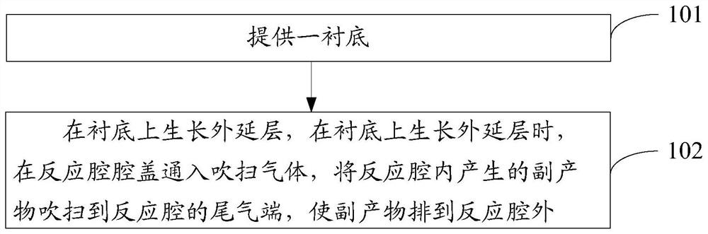
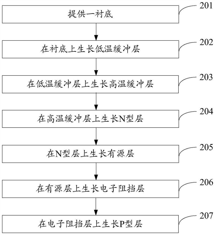
[0029] Step 101, providing a substrate.

[0030] Wherein, the substrate may be a sapphire substrate.

[0031] Step 102, grow the epitaxial layer on the substrate. When growing the epitaxial layer on the substrate, a purge gas is introduced into the cover of the reaction chamber to sweep the by-products generated in the reaction chamber to the tail gas end of the reaction chamber, so that the by-products The product is discharged out of the reaction chamber.

[0032] In this embodiment, the epitaxial layer includes a low-temperatur...


PUM

PropertyMeasurementUnit
thicknessaaaaaaaaaa
thicknessaaaaaaaaaa
thicknessaaaaaaaaaa

Abstract

The invention provides a growth method of a miniature light-emitting diode epitaxial wafer. The growth method comprises the following steps: growing an epitaxial layer on a substrate; when an epitaxial layer is grown on the substrate, introducing blowing gas into a cavity cover of the reaction cavity to blow by-products generated in the reaction cavity to the tail gas end of the reaction cavity, so that the by-products are discharged out of the reaction cavity; wherein the usage amount of the purge gas is positively related to the usage amount of an MO source required by growth of each layer,the flow of reaction gas required by growth of each layer, the growth thickness of each layer and the doping concentration of each layer; wherein the usage amount of the purge gas is also related to the growth stage of each layer of the epitaxial layer, the growth stage of each layer of the epitaxial layer is divided into an initial growth stage, an intermediate growth stage and an end growth stage, and the usage amount of the purge gas in the intermediate growth stage is greater than the usage amount of the purge gas in the initial growth stage and the end growth stage. The growth method canreduce the generation of surface particles in the growth process of the epitaxial wafer, forms an excellent surface, and guarantees the light-emitting effect of the miniature light-emitting diode.

Description

technical field [0001] The present disclosure relates to the technical field of semiconductors, in particular to a method for growing micro-LED epitaxial wafers. Background technique [0002] A light-emitting diode (English: Light Emitting Diode, referred to as: LED) is a semiconductor electronic component that can emit light. As an efficient, environmentally friendly and green new solid-state lighting source, LED is a new generation of light source with broad prospects, and is being rapidly and widely used in traffic lights, car interior and exterior lights, urban landscape lighting, indoor and outdoor display screens and small-pitch displays. screen and other fields. [0003] The epitaxial wafer is the primary product in the LED manufacturing process. In related technologies, when growing LED epitaxial wafers, the usual method is: provide a substrate, and grow a low-temperature buffer layer, a high-temperature buffer layer, an N-type layer, an active layer, an electron b...

Claims


Application Information

Patent Timeline
Patent Type & Authority Applications(China)
IPC IPC(8): H01L33/00C23C16/44
CPCC23C16/4408H01L33/005H01L33/007
Inventor 姚振从颖董彬忠李鹏
Owner HC SEMITEK SUZHOU
Why Eureka
Try Eureka