


Quick Research
Generate reliable direction feasibility study reports for your R&D in just a few steps.

Technical Q&A
Discover and master advanced knowledge NOW. Basics, ideas, possibilities, all at once.

Find Solutions
As an expert in R&D theories, this can generate solutions to your technical problems instantly.

Evaluate Feasibility
Analyze your overall solution with one click, know your potential R&D risks in advance.

Monitor Landscape
Get weekly tech updates, stay abreast of the latest tech innovations and key insights.
Vapor deposition apparatus and method for producing organic electronic device
A technology of evaporation and organic materials, applied in the direction of electric solid devices, electrical components, vacuum evaporation plating, etc., can solve the problem of not further accommodating large components, and achieve the effect of reducing the risk of adverse effects, reducing losses, and reducing burdens
- Summary
- Abstract
- Description
- Claims
- Application Information
AI Technical Summary
Problems solved by technology
Method used
Image


Examples
Embodiment 1
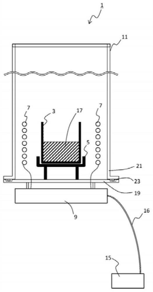
[0061] figure 1 A partial cross-sectional view of the vapor deposition device 1 (an example of the "vapor deposition device" in the claims of the present invention) of Example 1 is shown. The vapor deposition device 1 has: a container 3 (an example of a "container" in the claims of the present invention), a container holder 5, a coil 7 (an example of a "coil" in the claims of the present invention), a power semiconductor 9 (an example of a "coil" in the claims of the present invention), An example of the required "power semiconductor", a vacuum chamber 11 (an example of the "vacuum chamber" in the claims of the present invention), a DC power supply 15 (an example of the "DC power supply" in the claims of the present invention), and cable16. The container 3 is used to accommodate the organic material 17 . The container holder 5 is used to hold the container 3 . The coil 7 is wound around the container 3 . The power semiconductor 9 is electrically connected to the DC power ...
Embodiment 2
[0079] Image 6 It is a cross-sectional view showing a part of the vapor deposition device 61 of Example 2. The vapor deposition device 61 has a container 63 , a coil 65 , a power semiconductor 67 , a vacuum chamber 69 , a DC power supply 71 , and a cable 73 . The main difference between the vapor deposition device 61 and the vapor deposition device 1 is that the coil 65 is arranged outside the vacuum chamber 69 .
[0080] Specifically, the vacuum chamber 69 includes a chamber bottom 75 and a chamber upper 77 . The chamber bottom 75 is connected to the chamber top 77 by an O-ring 79 connection. The container 63 for storing the organic material 81 is arranged inside the chamber bottom 75 . Furthermore, the coil 65 surrounds the container 63 from the outside of the chamber bottom 75 .
[0081] like Image 6 As shown, the coil 65 and the container 63 pass through the structure separated by the vacuum chamber 69, and the organic material 81 will no longer adhere to the coil 6...
Embodiment 3
[0094] Next, refer to Figure 12 and Figure 13 , in this embodiment, the heating control by frequency control will be described. Figure 12 It is a graph showing the relationship between the AC frequency flowing into the coil and the input energy. Figure 13 It is a graph showing the relationship between the frequency range and the heating temperature.
[0095] like Figure 12 As shown in the schematic diagram, the maximum reachable temperature changes by frequency control using a frequency control unit such as a function generator. This demonstrates that heating control becomes possible by performing frequency control.
[0096] Furthermore, the control of voltage and current can only be controlled linearly in the past, but the present invention can perform nonlinear control through frequency control. Specifically, as Figure 13 As shown in the schematic diagram, in the frequency range near the resonance frequency, the maximum attained temperature changes only slightly ...
PUM
 Abstract
Description
Claims
Application Information
 - R&D Engineer
- R&D Manager
- IP Professional
- Industry Leading Data Capabilities
- Powerful AI technology
- Patent DNA Extraction
Browse by: Latest US Patents, China's latest patents, Technical Efficacy Thesaurus, Application Domain, Technology Topic, Popular Technical Reports.
© 2024 PatSnap. All rights reserved.Legal|Privacy policy|Modern Slavery Act Transparency Statement|Sitemap|About US| Contact US: help@patsnap.com