Wafer assembly with alignment marks, method for forming same, and method for aligning wafers

A technology for aligning marks and aligning marks, applied in the direction of electrical components, semiconductor devices, electric solid devices, etc., to achieve the effects of improving pattern clarity, solving bonding gaps, and improving bonding accuracy

Active Publication Date: 2022-01-28
WUHAN XINXIN SEMICON MFG CO LTD
View PDF12 Cites 0 Cited by
  • Summary
  • Abstract
  • Description
  • Claims
  • Application Information

AI Technical Summary

Problems solved by technology

[0005] The object of the present invention is to provide a wafer assembly with alignment marks, its forming method, and wafer alignment method, which can improve the recognition ability of alignment marks, eliminate overlay accuracy errors between different layers, and improve pattern definition while Solving Bonding Void Issues

Method used


Image

  • Wafer assembly with alignment marks, method for forming same, and method for aligning wafers
  • Wafer assembly with alignment marks, method for forming same, and method for aligning wafers
  • Wafer assembly with alignment marks, method for forming same, and method for aligning wafers

Examples


Embodiment Construction

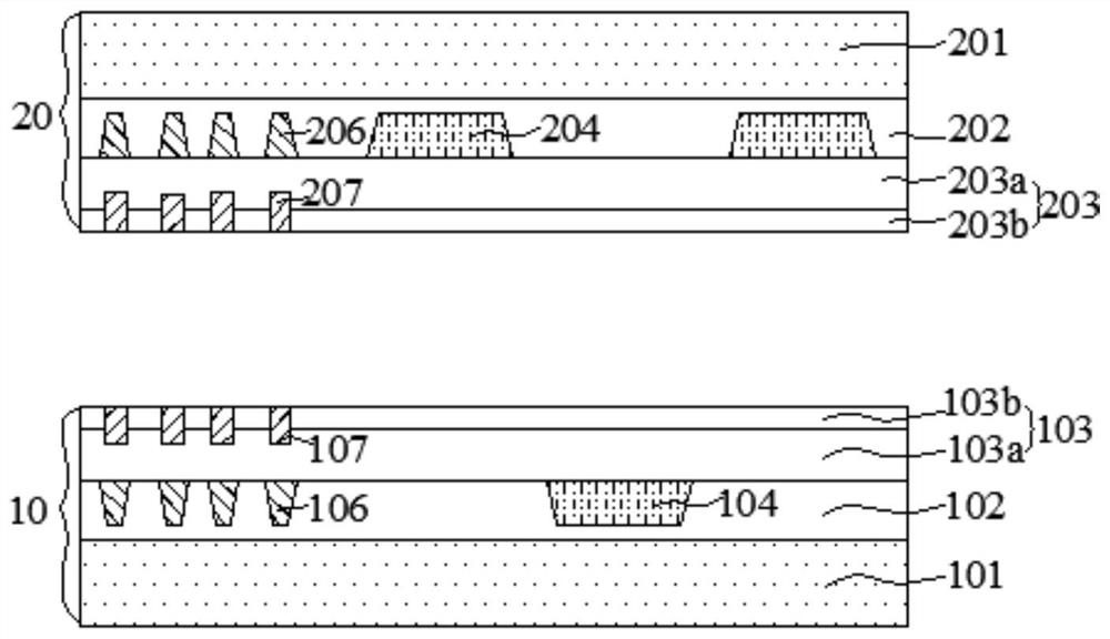
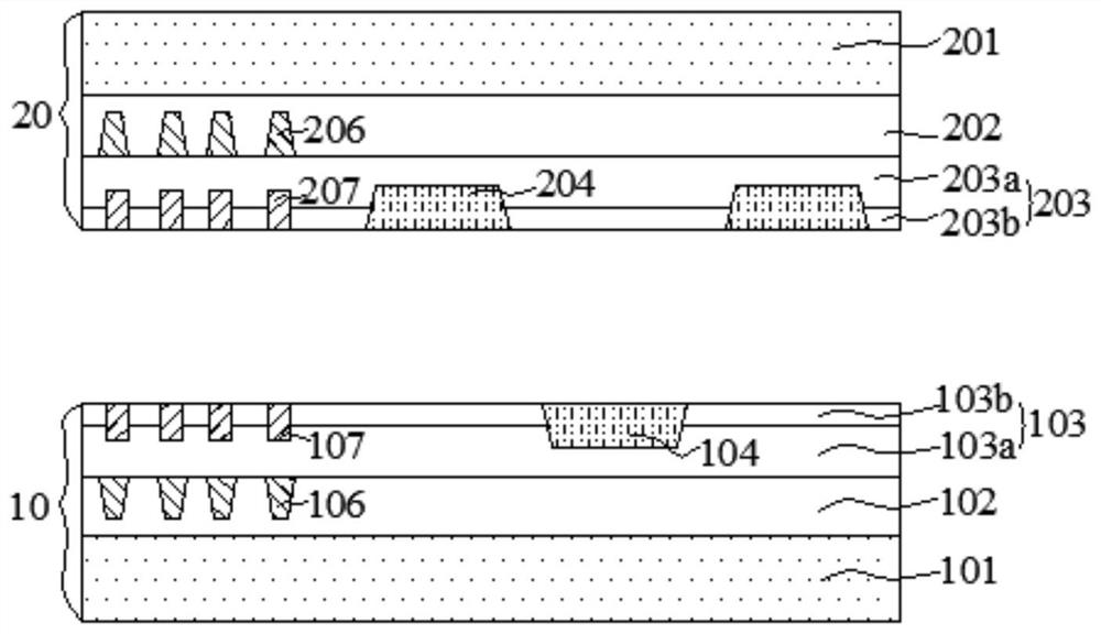
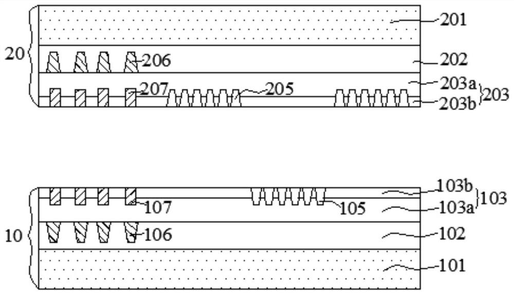
[0049] Embodiments of the present invention provide a wafer assembly with an alignment mark, a forming method thereof, and a wafer alignment method. The present invention will be described in further detail below in conjunction with the accompanying drawings and specific embodiments. The advantages and features of the present invention will become clearer from the following description. It should be noted that the drawings are all in a very simplified form and use imprecise scales, and are only used to facilitate and clearly assist the purpose of illustrating the embodiments of the present invention.

[0050] An embodiment of the present invention provides a wafer assembly with an alignment mark, including:

[0051] The first wafer, the first wafer includes a first substrate, a first dielectric layer on the first substrate, a first block mark embedded in the first dielectric layer, and a first block mark on the first substrate. The first bonding layer on the first dielectric...


PUM


Abstract

The present invention provides a wafer component with an alignment mark, its forming method, and a wafer alignment method. The alignment mark is distributed in the bonding layer and the dielectric layer of the first wafer and the second wafer, and the first In the wafer, the reflected light of the first dot-shaped mark and the first block-shaped mark are superimposed to ensure the pattern definition of the alignment mark. The first dot-shaped mark is located in the first bonding layer, and the second The upper surface of the dot-shaped mark is flush with the upper surface of the first bonding layer, and the first dot-shaped mark on the bonding surface ensures microscopic flatness, and there is no gap after bonding; at the same time, the first dot-shaped mark on the bonding surface The first dot mark also eliminates the overlay accuracy error between different layers. The second wafer is the same as the first wafer. The use of the alignment mark on the bonding machine can not only eliminate the overlay accuracy error between different layers, improve the definition of the pattern, but also solve the problem of bonding voids.

Description

technical field [0001] The invention belongs to the technical field of integrated circuit manufacturing, and in particular relates to a wafer component with an alignment mark and a forming method thereof. Background technique [0002] With the development of semiconductor VLSI, three-dimensional stacked packaging technology stacks silicon wafers through bonding technology to realize a metal interconnection structure on a three-dimensional level, which can reduce interconnection distances, increase transmission speeds, and reduce device volume. [0003] Wafer bonding technology is one of the important means to realize three-dimensional stacking. Wafer bonding technology includes hybrid bonding of metal layer to metal layer and dielectric layer to dielectric layer. Hybrid bonding can provide metal interconnection structure and sufficient mechanical support at the same time, and is one of the key technologies of three-dimensional stacking. [0004] When the upper and lower waf...

Claims


Application Information

Patent Timeline
Patent Type & Authority Patents(China)
IPC IPC(8): H01L23/544H01L29/06H01L21/68
CPCH01L23/544H01L29/06H01L21/681H01L2223/54426H01L2223/54453
Inventor 叶国梁胡杏易洪昇
Owner WUHAN XINXIN SEMICON MFG CO LTD
Why Eureka
Try Eureka