Multi-junction solar cell
A technology of solar cells and sub-cells, applied in circuits, photovoltaic power generation, electrical components, etc., can solve problems such as voltage loss, and achieve the effect of high lateral conductivity and small loss
- Summary
- Abstract
- Description
- Claims
- Application Information
AI Technical Summary
Problems solved by technology
Method used
Image
Examples
Embodiment Construction
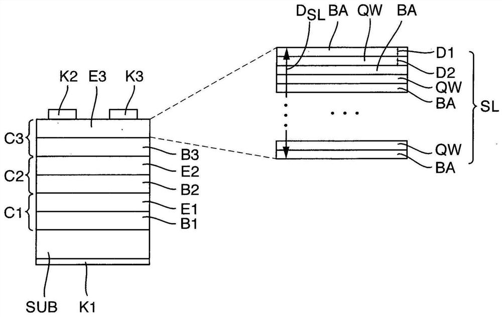
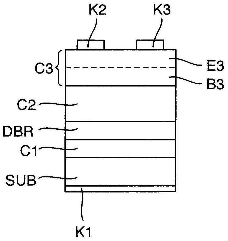
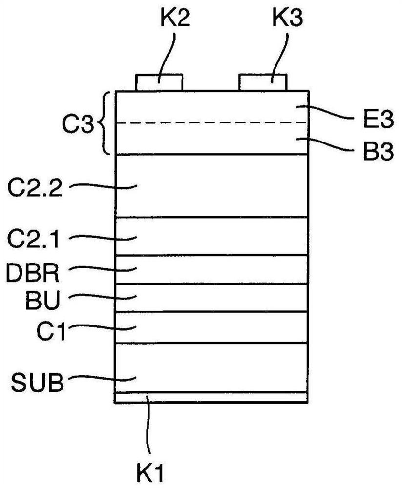
[0056] figure 1 The image in shows a view of a first embodiment of a stacked multi-junction solar cell MJ comprising a stack consisting of a substrate layer SUB, a lowermost subcell C1, a middle subcell C2 and an uppermost subcell C3 ST. A flat connection layer K1 is formed on the underside of the stack ST. Connecting fingers K2 , K3 are arranged on the upper side of the stack.
[0057] Each sub-cell C1, C2, and C3 has a base B1, B2, B3 and an emitter E1, E2, E3, respectively, wherein the emitter E3 and the base B3 of the uppermost sub-cell C3 are made of III-V semiconductor materials composition.
[0058] The emitter E3 of the uppermost sub-cell C3 comprises a superlattice SL. The superlattice includes a plurality of thin well layers QW with a thickness of D2 and a plurality of thin barrier layers BA with a thickness of D1, wherein the well layers QW and the barrier layers BA are alternately stacked on each other. The total thickness D of the superlattice SL From the th...
PUM
| Property | Measurement | Unit |
|---|---|---|
| thickness | aaaaa | aaaaa |
Abstract
Description
Claims
Application Information
 - R&D
- Intellectual Property
- Life Sciences
- Materials
- Tech Scout
- Unparalleled Data Quality
- Higher Quality Content
- 60% Fewer Hallucinations
Browse by: Latest US Patents, China's latest patents, Technical Efficacy Thesaurus, Application Domain, Technology Topic, Popular Technical Reports.
© 2025 PatSnap. All rights reserved.Legal|Privacy policy|Modern Slavery Act Transparency Statement|Sitemap|About US| Contact US: help@patsnap.com


