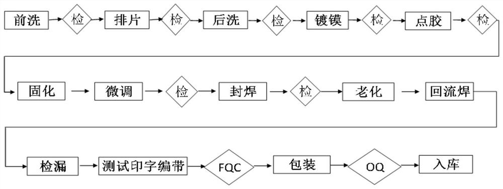
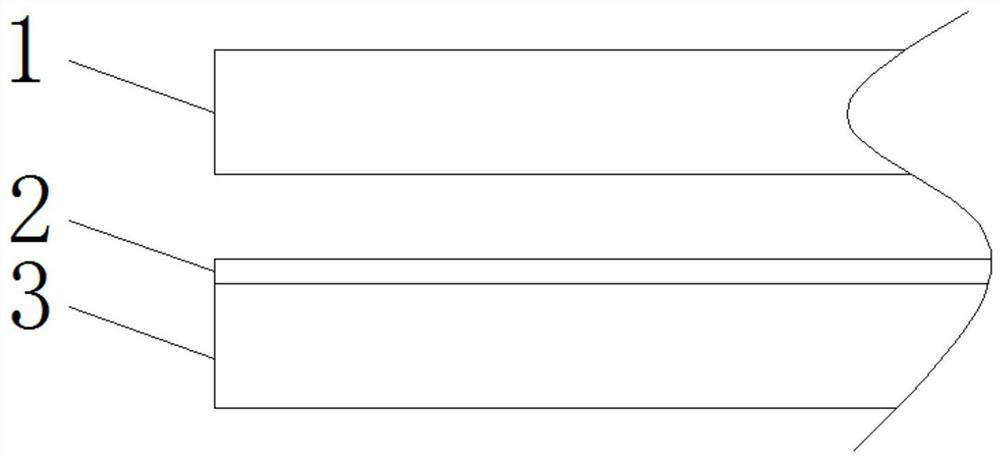
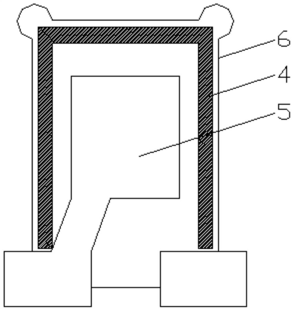
Manufacturing process of SMD2016high fundamental frequency resonator
A technology of SMD2016 and manufacturing process, applied to electrical components, impedance networks, etc., can solve the problems of unsuitable 5G communication equipment, slow frequency scanning operation speed, high price, etc., to avoid chip running, solve chip layout, and avoid deformation Effect
- Summary
- Abstract
- Description
- Claims
- Application Information
AI Technical Summary
Problems solved by technology
Method used
Image
Examples
Embodiment 1
[0043] Design and manufacture 2016 / 80.000MHz / 9pF high fundamental frequency crystal resonator, the specifications require FL:±10ppm; C0:1.05±0.2Pf; C1:3.5±0.5pF; RR<30Ω, combined with the formula C0=0.0402×A×f standard ÷K+(0.2~0.6), match the size of the design positioning sheet, upper mask plate and lower mask plate as follows:
[0044] Positioning piece: 2016 / 672 bits / A2615 / 1.31*0.91*0.13mm
[0045] Upper mask plate: B2604 UP MASK / 0.70*0.60*0.08mm, convex layer thickness 0.05mm
[0046] Lower mask: B2604 DN MASK / 0.70*0.60*0.08mm, convex layer thickness 0.05mm.
[0047] According to the design of the present invention, mass production can meet the specification conditions, and the normal temperature data are as follows:
[0048]
[0049] Drop reliability test standard: drop 6 times from a height of 150cm, no fragments, ΔFL<3ppmΔRR<3Ω, the comparison data are as follows:
[0050]
Embodiment 2
[0051] Example 2: Design and manufacture of 2016 / 96.000MHz / 9pF high fundamental frequency crystal resonator, specifications require FL: ±10ppm; C0:0.85±0.1Pf; C1:3±0.5pF; RR<20Ω, combined with the formula C0=0.0402× A × f standard ÷ K + (0.2 ~ 0.6), wafer design size: 0.787 * 0.611 * 0.017, matching the design of the plated jig, the dimensions of the positioning piece, upper mask plate, and lower mask plate are as follows:
[0052] Positioning piece: 672 bits / A1607 / 1.07*0.69*0.12mm
[0053] Upper mask plate: B1607 UP MASK / 0.50*0.50*0.08mm, convex layer thickness 0.05mm
[0054] Lower mask: B1607 DN MASK / 0.50*0.50*0.08mm, convex layer thickness 0.05mm.
[0055] According to the design of the present invention, mass production can meet the specification conditions, and the normal temperature data are as follows:
[0056]
[0057]
[0058] Drop reliability test standard: drop 6 times from a height of 150cm, no fragments, ΔFL<3ppm, ΔRR<3Ω, the comparison data are as follow...
PUM
| Property | Measurement | Unit |
|---|---|---|
| length | aaaaa | aaaaa |
| width | aaaaa | aaaaa |
| length | aaaaa | aaaaa |
Abstract
Description
Claims
Application Information
 - R&D Engineer
- R&D Manager
- IP Professional
- Industry Leading Data Capabilities
- Powerful AI technology
- Patent DNA Extraction
Browse by: Latest US Patents, China's latest patents, Technical Efficacy Thesaurus, Application Domain, Technology Topic, Popular Technical Reports.
© 2024 PatSnap. All rights reserved.Legal|Privacy policy|Modern Slavery Act Transparency Statement|Sitemap|About US| Contact US: help@patsnap.com


