LED flip chip packaging device and packaging process thereof

A technology for packaging devices and flip-chips, which is applied to semiconductor devices, electrical components, circuits, etc., can solve the problems of low error tolerance, difficulty in controlling the position of glue points, positioning deviation, etc., achieve strong antistatic ability, improve the gathering effect, The effect of reducing production costs

Pending Publication Date: 2020-10-16
HARVATEK OPTOELECTRONICS SHENZHEN
View PDF0 Cites 1 Cited by
  • Summary
  • Abstract
  • Description
  • Claims
  • Application Information

AI Technical Summary

Problems solved by technology

The LED flip chip in the above patent has the following disadvantages: the connection method of bonding is used, which leads to a low error tolerance rate, and it is difficult to control the position of the glue point, which is easy to cause positioning deviation

Method used


Image

  • LED flip chip packaging device and packaging process thereof
  • LED flip chip packaging device and packaging process thereof
  • LED flip chip packaging device and packaging process thereof

Examples


Embodiment 1

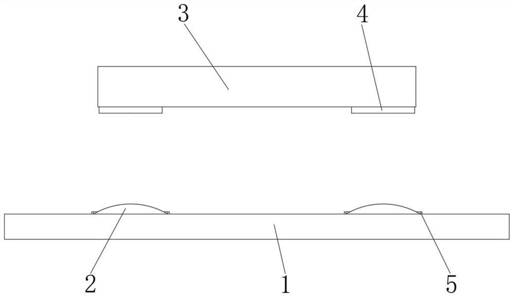
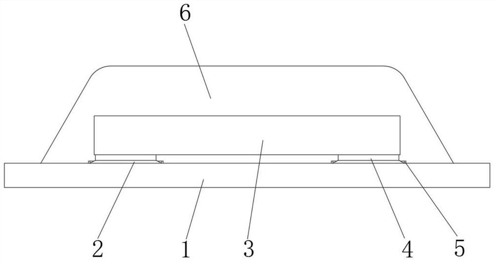
[0033] A kind of LED flip-chip packaging device, such as figure 1 , figure 2 As shown, it includes a substrate 1 and a chip 3; the substrate 1 is provided with copper foil, the copper foil is plated with 10u of silver, the top outer wall of the substrate 1 is provided with a limiting ring 5, and the top outer wall of the substrate 1 in the limiting ring 5 Tin spots 2 are soldered on the top; solder spots 4 are provided on the surface of the chip 3, and the solder spots 4 of the chip 3 are reflow-welded in the limiting ring 5 on the substrate 1 through the tin spots 2; the positions of the limiting ring 5 and the tin spots 2 and The quantity is adapted to the soldering point 4; the chip 3 is coated with an adhesive layer 6, and the adhesive layer 6 is completely wrapped around the chip 3 and the limit ring 5; in this embodiment, the chip 3 is set to pass through the soldering point 4 and the tin point 2 Reverse soldering on the substrate 1 does not require any baking or wire ...

Embodiment 2

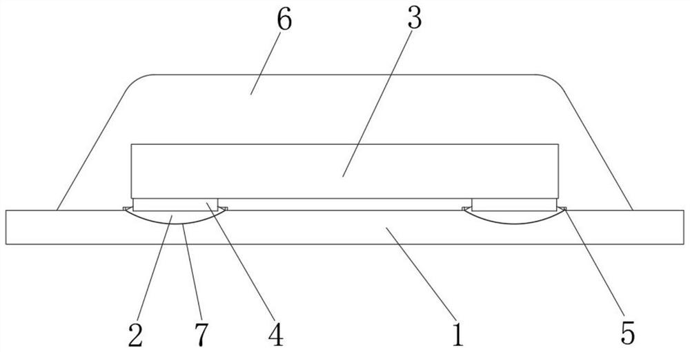
[0037] A kind of LED flip-chip packaging device, such as image 3 As shown, in order to further improve the welding firmness; this embodiment makes the following improvements on the basis of embodiment 1: the outer wall of the top of the substrate 1 is processed with a tin groove 7, and the tin point 2 is welded in the tin groove 7 on the substrate 1, The cross section of the tin bath 7 is an arc-shaped structure; by setting the tin bath 7, it can benefit the substrate 1 to eat tin, and improve the gathering effect of the tin spot 2, further avoiding the leakage of the tin spot 2, and ensuring the welding quality.

[0038] In order to improve reliability, such as image 3 As shown, the maximum diameter of the tin bath 7 is larger than the diameter of the solder joint 4 .

Embodiment 3

[0040] A kind of LED flip-chip packaging device, such as Figure 4 As shown, in order to improve the tightness of the adhesive layer 6; this embodiment makes the following improvements on the basis of embodiment 2: the outer wall of the top of the substrate 1 is processed with a glue groove 8, and the glue groove 8 is located outside the chip 3 and the limit ring 5 , the edge of the glue layer 6 is completely filled inside the glue groove 8; by setting the glue groove 8, the firmness of the connection between the edge of the glue layer 6 and the substrate 1 can be improved, thereby improving the adhesive layer 6 for the chip 3, etc. The sealing performance of the structure.


PUM


Abstract

The invention discloses an LED flip chip packaging device and a packaging process thereof, which relate to the technical field of LED flip chip packaging. The LED flip chip packaging device specifically comprises a substrate and a chip, wherein the substrate is provided with a copper foil, the copper foil is plated with 10u silver, the outer wall of the top of the substrate is provided with a limiting ring, and tin points are welded on the outer wall of the top of the substrate in the limiting ring; and welding points are arranged on the surface of the chip. The packaging process comprises thefollowing steps of preparing: preparing a chip to be welded, and preparing a substrate with a limiting ring corresponding to the chip, and die bonding: dispensing a tin point in the limiting ring onthe substrate, fixing the flip chip on the substrate, and enabling the welding point to correspond to the tin point in position. The chip is reversely welded on the substrate through the welding points and the tin points, no baking or wire welding is needed after die bonding is completed, reflow soldering is directly carried out, and the production efficiency is improved; due to the arrangement ofthe limiting ring, tin points and welding points can be conveniently positioned.

Description

technical field [0001] The invention relates to the technical field of LED flip-chip packaging, in particular to an LED flip-chip packaging device and a packaging process thereof. Background technique [0002] At present, the high-power LED flip-chip packaging process has become more popular, mainly because the chip size is large, and the process is relatively easy to implement; while the low-power flip-chip process is rare, such as 1206, 0805, 0603, 0402 and other chip-type low-power LEDs, due to The size of the chip is small, the size of the chip is smaller, and the packaging process is extremely difficult. At present, the chip-type low-power LED flip-chip technology such as 1206, 0805, 0603, and 0402 is still blank in the market. [0003] The prior art discloses an LED flip chip solid crystal conductive bonding structure, which includes an LED flip chip and an electronic circuit board. The lower surface of the LED flip chip is sequentially provided with LED flip chip cath...

Claims


Application Information

Patent Timeline
Patent Type & Authority Applications(China)
IPC IPC(8): H01L33/48H01L33/52H01L33/62
CPCH01L33/48H01L33/52H01L33/62H01L2933/0033H01L2933/005H01L2933/0066
Inventor 梁明清
Owner HARVATEK OPTOELECTRONICS SHENZHEN
Why Eureka
Try Eureka