A display panel and its manufacturing method, and a display device
A display panel and display area technology, which is applied in the direction of final product manufacturing, sustainable manufacturing/processing, semiconductor/solid-state device manufacturing, etc., can solve problems such as the inability to realize a full screen, ensure normal use performance, and reduce diffraction coherent superposition phenomenon , the effect of increasing the effective light transmission area
- Summary
- Abstract
- Description
- Claims
- Application Information
AI Technical Summary
Problems solved by technology
Method used
Image
Examples
Embodiment 1
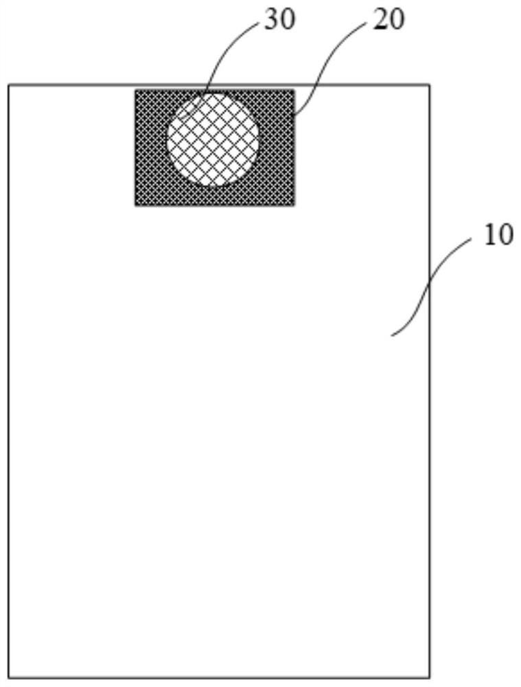
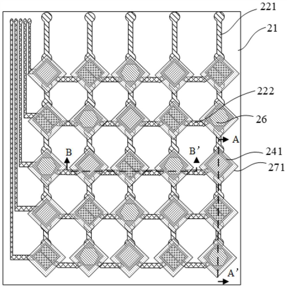
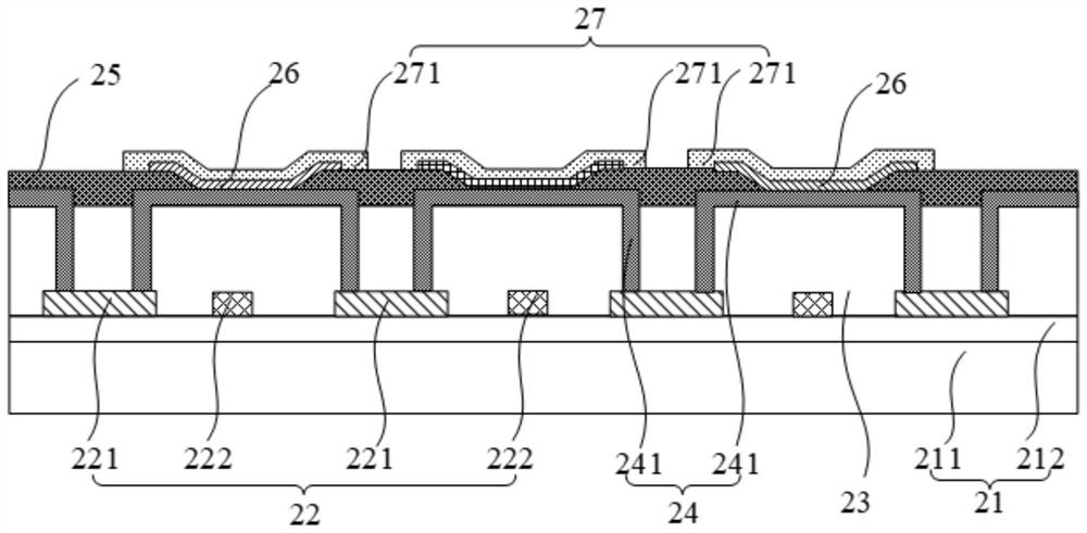
[0053] refer to figure 1 , showing a schematic diagram of a display panel according to an embodiment of the present invention, figure 2 A plan view of a functional display area in a display panel according to an embodiment of the present invention is shown, image 3 show figure 2 Shown is a cross-sectional view of the display panel along section A-A', Figure 4 show figure 2 A cross-sectional view of the display panel along section B-B' is shown.
[0054] An embodiment of the present invention provides a display panel, comprising: a substrate 21, the substrate 21 is divided into an effective display area 10 and a functional display area 20 where functional devices 30 are located; The electrode connection layer 22, the electrode connection layer 22 includes a plurality of mutually insulated anode connection lines 221 and cathode connection lines 222, and the anode connection lines 221 are distributed along the first direction, and the cathode connection lines 222 are dis...
Embodiment 2
[0098] refer to Image 6 , showing a flowchart of a method for manufacturing a display panel according to an embodiment of the present invention, which may specifically include the following steps:
[0099] Step 601, providing a substrate; the substrate is divided into an effective display area and a functional display area where functional devices are located.
[0100]In the embodiment of the present invention, first, a substrate 21 is fabricated, and the substrate 21 is divided into an effective display area 10 and a functional display area 20 where the functional device 30 is located.
[0101] Specifically, an active layer, a gate insulating layer and a gate layer are respectively formed on the effective display area 10 of the substrate 211, and then, an interlayer dielectric layer is formed on both the effective display area 10 and the functional display area 20, and then, in the effective display area A source-drain electrode layer is formed on the interlayer dielectric ...
Embodiment 3
[0128] An embodiment of the present invention provides a display device including a functional device 30 and the above-mentioned display panel; the functional device 30 is disposed on the side of the substrate 21 away from the electrode connection layer 22 , and the functional device 30 is located in the functional display area 20 .
[0129] The functional device 30 includes a camera, a sensor and other devices.
[0130] For the specific description of the display panel, reference may be made to the description of the first embodiment and the second embodiment, which is not repeated in this embodiment of the present invention.
[0131] In addition, the display device further includes a driver chip, a TCON (Timer Control Register, timing controller) and other devices.
[0132] In practical applications, the display device may be any product or component with a display function, such as a mobile phone, a tablet computer, a monitor, a notebook computer, and a navigator.
[0133]...
PUM
 Abstract
Description
Claims
Application Information
 - R&D
- Intellectual Property
- Life Sciences
- Materials
- Tech Scout
- Unparalleled Data Quality
- Higher Quality Content
- 60% Fewer Hallucinations
Browse by: Latest US Patents, China's latest patents, Technical Efficacy Thesaurus, Application Domain, Technology Topic, Popular Technical Reports.
© 2025 PatSnap. All rights reserved.Legal|Privacy policy|Modern Slavery Act Transparency Statement|Sitemap|About US| Contact US: help@patsnap.com


