
A method for automatic generation of precise 3D model of PCBA based on ecad interface

A 3D model and automatic generation technology, applied in 3D modeling, database model, structured data retrieval, etc., can solve the inconsistency between the calling model and the actual device, the deviation of key parameters such as device height, the degree of model restoration and the limitation of usability, etc. problems, to achieve the effect of improving design accuracy and review efficiency, and ensuring uniqueness

Active Publication Date: 2020-12-04
CHENGDU ZHIMINGDA DIGITAL EQUIP
View PDF10 Cites 0 Cited by
  • Summary
  • Abstract
  • Description
  • Claims
  • Application Information

AI Technical Summary

Problems solved by technology

[0008] Problem a: Since this method calls the ECAD device model based on the device package name, it is impossible to call the device differently for the same package corresponding to multiple devices of different sizes, resulting in large deviations in key parameters such as device height;
[0009] Problem b: The ECAD device model only includes simple package envelope size information, which cannot accurately express the device appearance and detail size, and the model restoration degree and usability are limited
[0010] Based on the above problems, the industry has gradually developed an improved method, which is to establish a device model library based on the package name in the 3D design software according to the appearance and actual size of the device, and add the ECAD model library to the configuration file of the 3D design software. Retrieval path, retrieve and call the device model library through the device package name information in the EMN file and combine the EMP file to generate a PCBA 3D model with a high degree of restoration. This method solves problem b in the traditional method, but cannot solve problem a, which still exists The components that share the package cannot be correctly represented, and the calling model does not match the actual components. The PCBA 3D model generated by this improved method can only be regarded as a rough model.

Method used


Image

  • A method for automatic generation of precise 3D model of PCBA based on ecad interface

Examples


Embodiment Construction

[0032] The following will clearly and completely describe the technical solutions in the embodiments of the present invention with reference to the accompanying drawings in the embodiments of the present invention. Obviously, the described embodiments are only some, not all, embodiments of the present invention. Based on the embodiments of the present invention, all other embodiments obtained by persons of ordinary skill in the art without making creative efforts belong to the protection scope of the present invention.

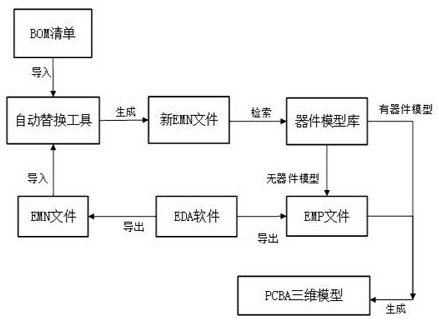
[0033] see figure 1 , the present invention provides a technical solution: a method for automatically generating a precise three-dimensional model of a PCBA based on an ECAD interface, including an EMN file and a BOM list; wherein,

[0034] The EMN file is used to record the geometric coordinate information of the PCB board and the packaging name, bit number and coordinate information of each device on the board;

[0035] The BOM list is used to reflect the i...


PUM


Abstract

The invention discloses a PCBA accurate three-dimensional model automatic generation method based on an ECAD interface, and relates to the technical field of three-dimensional model automatic generation methods, including an EMN file and a BOM list. The EMN file is used for recording geometric coordinate information of the PCB and packaging names, bit numbers and coordinate information of all devices on the board; the BOM list is used for reflecting information of material codes, material description, specifications and models, quantity and bit numbers; the beneficial effects of the inventionare that a device bit number in the EMN file is exported through EDA software and associated with the device bit number with device information in the BOM list, and a packaging name in the EMN file is replaced with a device code; the uniqueness of the device corresponding to the EMN file information is ensured, so that the device model library can be retrieved through the device code, the devicemodel can be accurately called, the PCBA accurate three-dimensional model based on the ECAD interface can be automatically generated, and the design accuracy and the evaluation efficiency of a high-density electronic product can be greatly improved.

Description

technical field [0001] The invention relates to the technical field of automatic three-dimensional model generation methods, in particular to a method for automatic generation of accurate three-dimensional models of PCBA based on ECAD interfaces. Background technique [0002] In recent years, with the rapid development of the electronic communication industry, products are increasingly pursuing miniaturization and high integration in form, and the requirements for structural space utilization are getting higher and higher. In the process of electronic product design, it is necessary to establish as accurate a PCBA three-dimensional Model, in order to guide scheme design, layout optimization and interference check. [0003] The current mainstream EDA software on the market can export EMN and EMP files, which contain the following information: [0004] EMN file——Record the geometric coordinate information of the PCB board and the package name, bit number and coordinate inform...

Claims


Application Information

Patent Timeline
Patent Type & Authority Patents(China)
IPC IPC(8): G06T17/00G06F16/28
CPCG06T17/00G06F16/284
Inventor 杜璟明刘波赵薇娜李渊
Owner CHENGDU ZHIMINGDA DIGITAL EQUIP
Learn More