Reverse electrowetting mechanical energy collection device and mechanical energy collection device
A technology of collecting device and mechanical energy, applied in capacitors, capacitors whose capacitance is changed mechanically, and electrical components, etc., can solve problems such as insufficient energy collection efficiency, avoid charge trapping, improve functional characteristics, and improve energy generation efficiency. Effect
- Summary
- Abstract
- Description
- Claims
- Application Information
AI Technical Summary
Problems solved by technology
Method used
Image
Examples
Embodiment 1
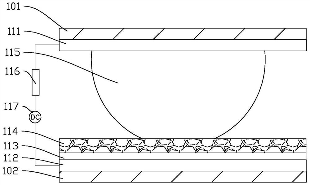
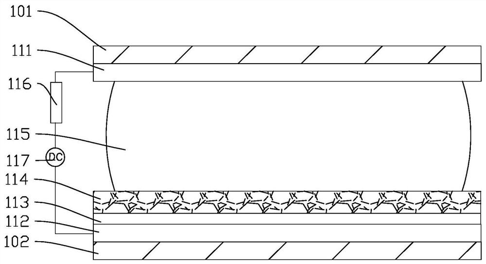
[0028] refer to figure 1 , shows a schematic structural view of the reverse electrowetting mechanical energy harvesting device of Example 1 of the present invention when no external mechanical force is applied. The reverse electrowetting mechanical energy harvesting device includes a first electrode substrate and a second electrode substrate oppositely arranged, the first electrode substrate includes a first substrate 101 and a first electrode layer 111, and the first electrode layer 111 is formed on the first substrate 101 close to One side of the second electrode substrate. The second electrode substrate includes a second substrate 102 and a second electrode layer 112 , and the second electrode layer 112 is formed on a side of the second substrate 102 close to the first electrode substrate. An accommodating chamber is formed between the first electrode substrate and the second electrode substrate, and in the accommodating chamber, the side of the second electrode substrate ...
Embodiment 2
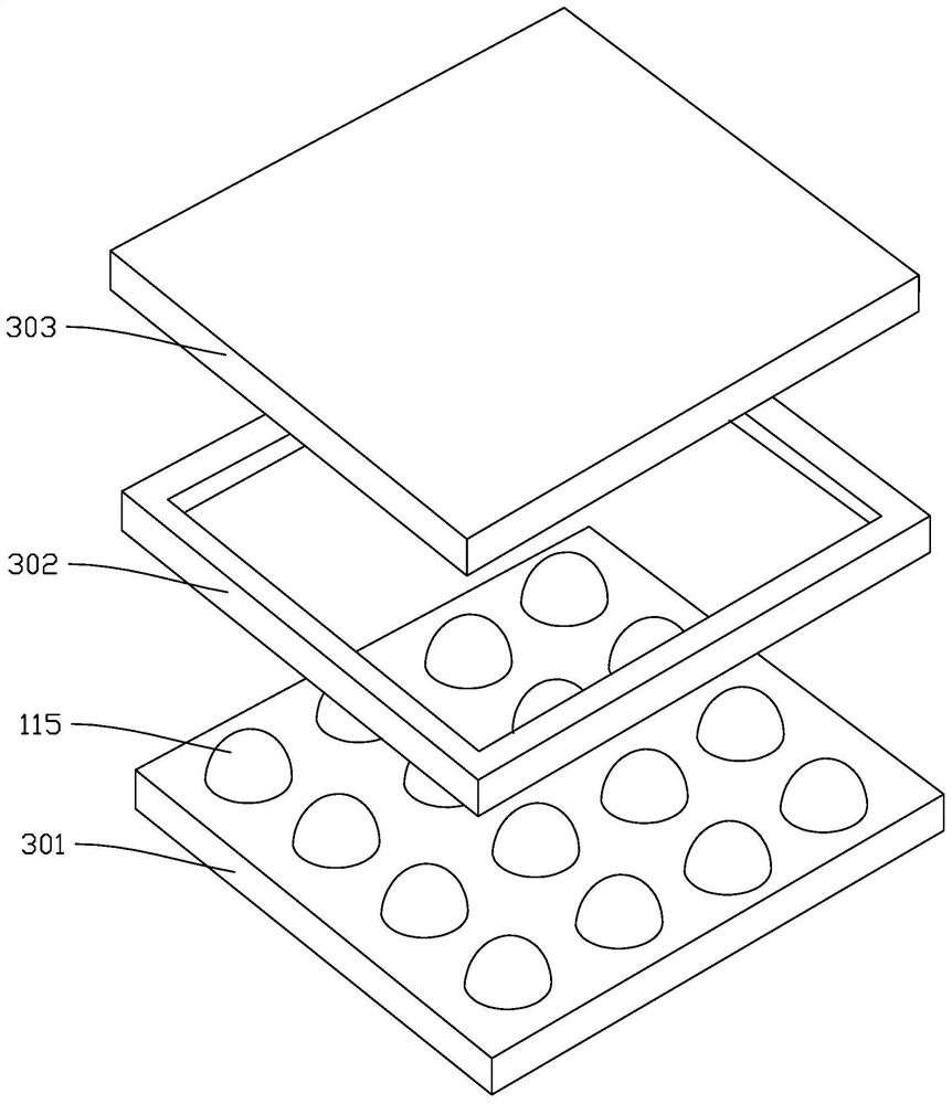
[0034] refer to image 3 , image 3 It is a structural schematic diagram of the mechanical energy harvesting device of Embodiment 2 of the present invention. The mechanical energy harvesting device includes a lower substrate 301 , an elastic packaging frame 302 , an upper substrate 303 and conductive liquid droplets 115 arranged in an array on the lower substrate 301 . The upper substrate 303 is a separate conductive substrate. The lower substrate 301 includes a conductive substrate, and a solid dielectric layer (not shown in the figure) and a liquid-injected smooth porous surface layer (not shown in the figure) are sequentially provided on the side of the conductive substrate close to the elastic packaging frame 302 . Wherein, the solid dielectric layer is a PTFE layer, and the liquid-injected smooth porous surface layer is in contact with the conductive liquid droplet 115 . The lower substrate 301 and the upper substrate 303 are also electrically connected with a DC volta...
Embodiment 3
[0036] Comparative Test
PUM
| Property | Measurement | Unit |
|---|---|---|
| thickness | aaaaa | aaaaa |
Abstract
Description
Claims
Application Information
 - Generate Ideas
- Intellectual Property
- Life Sciences
- Materials
- Tech Scout
- Unparalleled Data Quality
- Higher Quality Content
- 60% Fewer Hallucinations
Browse by: Latest US Patents, China's latest patents, Technical Efficacy Thesaurus, Application Domain, Technology Topic, Popular Technical Reports.
© 2025 PatSnap. All rights reserved.Legal|Privacy policy|Modern Slavery Act Transparency Statement|Sitemap|About US| Contact US: help@patsnap.com


