A light-emitting chip and a light-emitting module
A light-emitting chip and chip technology, which is applied in the direction of semiconductor devices, electrical components, circuits, etc., can solve the problems of circuit board thickness limitation and high cost of glass circuit boards, and achieve the effects of low processing cost, convenient production and simplified structure
- Summary
- Abstract
- Description
- Claims
- Application Information
AI Technical Summary
Problems solved by technology
Method used
Image

Examples
Embodiment 1
[0035] The embodiments of the present invention are mainly used to describe the basic structure of the light-emitting chip involved in the present invention.
[0036] An embodiment of the present invention provides a light-emitting chip. The light-emitting chip includes a chip body, a first electrode connection end, and a second electrode connection end. The chip body includes a first electrode layer and a second electrode layer that are insulated from each other. The first electrode connection end and the second electrode connection end are arranged at the bottom of the chip body, the first electrode connection end is electrically connected to the first electrode layer, and the second electrode connection end is connected to the The second electrode layer is electrically connected. Specifically, the present invention mainly improves the structure of the light-emitting chip based on the electrode connection end. Therefore, in the embodiment of the present invention, the compon...
Embodiment 2
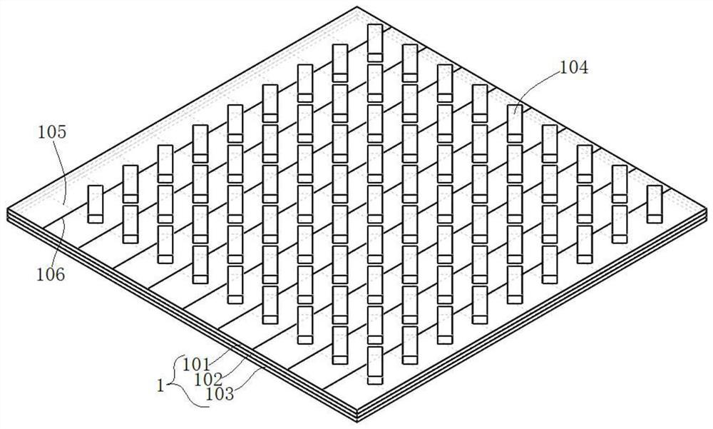
[0042] figure 2 A schematic diagram showing a three-dimensional structure of a light-emitting chip according to an embodiment of the present invention, image 3 A schematic cross-sectional structure diagram of a light-emitting chip according to an embodiment of the present invention is shown, wherein the cross-hatching lines are not shown.
[0043] An embodiment of the present invention provides a light-emitting chip. Basically, the light-emitting chip includes a chip body, a first electrode connection end, and a second electrode connection end, wherein the chip body has different structures according to different types of light-emitting chips, basically Yes, the chip body needs to be energized to achieve light emission. Commonly, the chip body includes a first electrode layer and a second electrode layer that are insulated from each other. The first electrode layer and the second electrode layer are respectively the two electrodes of the chip body (usually positive and nega...
Embodiment 3
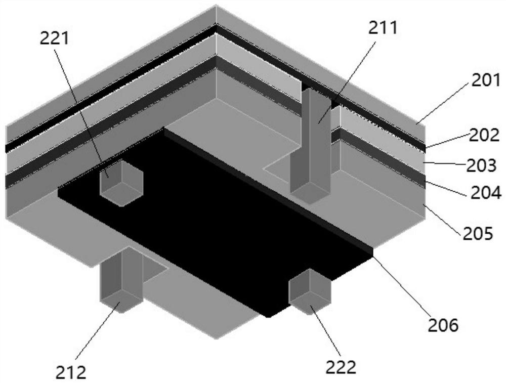
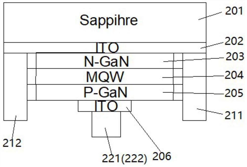
[0050] Figure 4 A schematic diagram showing a three-dimensional structure of a light-emitting chip according to an embodiment of the present invention, Figure 5 A schematic cross-sectional structure diagram of a light-emitting chip according to an embodiment of the present invention is shown, wherein the cross-hatching lines are not shown.
[0051] Specifically, different from the second embodiment, the first gallium nitride layer 402, the quantum well layer 404, the second gallium nitride layer 405 and the second electrode layer 406 of the light-emitting chip of the embodiment of the present invention are stacked in sequence, and the The first electrode layer 403 is embedded in the first gallium nitride layer 402; the second electrode layer 406 is located at the bottom of the chip body.
[0052] Further, the chip body further includes a sapphire layer 401, and the sapphire layer 401 is arranged on the top of the chip body.
[0053] On the basis of the light-emitting chip ...
PUM
| Property | Measurement | Unit |
|---|---|---|
| thickness | aaaaa | aaaaa |
Abstract
Description
Claims
Application Information
 - R&D
- Intellectual Property
- Life Sciences
- Materials
- Tech Scout
- Unparalleled Data Quality
- Higher Quality Content
- 60% Fewer Hallucinations
Browse by: Latest US Patents, China's latest patents, Technical Efficacy Thesaurus, Application Domain, Technology Topic, Popular Technical Reports.
© 2025 PatSnap. All rights reserved.Legal|Privacy policy|Modern Slavery Act Transparency Statement|Sitemap|About US| Contact US: help@patsnap.com