A wafer automatic loading device

An automatic, loading technology, used in transportation and packaging, discharge tubes, electrical components, etc., can solve the problems of affecting wafer quality, easy to scratch wafers, low wafer loading efficiency, etc., to achieve wafer quality and The pass rate is not affected, the loading efficiency is improved, and the parallel adjustment operation is simple and convenient.

Active Publication Date: 2020-10-16
SHANDONG NOVOSHINE OPTOELECTRONICS CO LTD
View PDF7 Cites 0 Cited by
  • Summary
  • Abstract
  • Description
  • Claims
  • Application Information

AI Technical Summary

Problems solved by technology

[0005] Specifically, the technical problem to be solved by the present invention is to provide an automatic wafer loading device to solve the technical problems of low efficiency of manual wafer loading, easy scratching of wafers and affecting the quality of wafers.

Method used


Image

  • A wafer automatic loading device
  • A wafer automatic loading device
  • A wafer automatic loading device

Examples


Embodiment Construction

[0045] The present invention will be further described below in conjunction with specific examples. However, the uses and purposes of these exemplary embodiments are only used to illustrate the present invention, and do not constitute any form of limitation to the actual protection scope of the present invention, nor limit the protection scope of the present invention thereto.

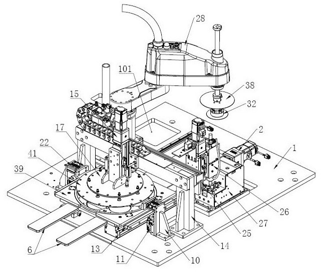
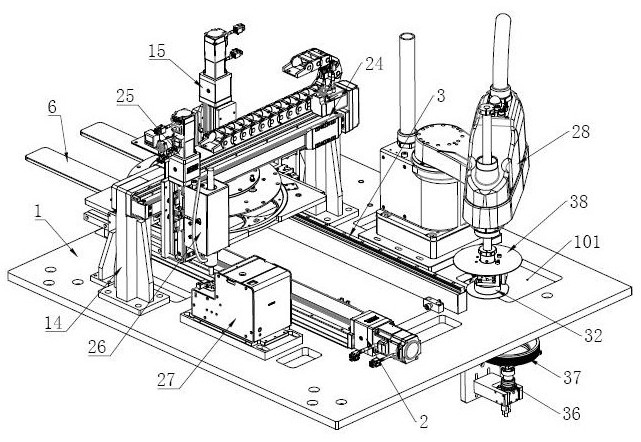
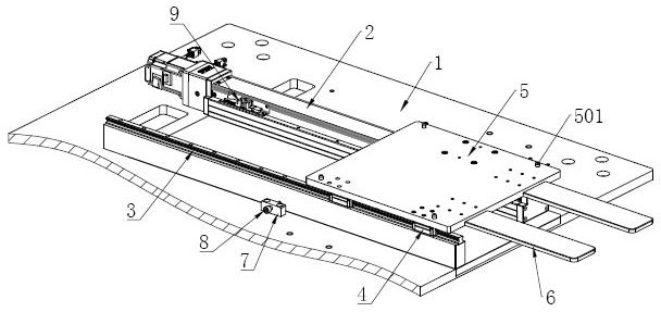
[0046] Such as Figure 1 to Figure 3 As shown, this embodiment provides an automatic wafer loading device, including a workbench 1, on which a positioning pallet 5 driven by a driving device is slidably installed, and the upper surface of the positioning pallet 5 is provided with several The locating pin 501 that realizes the positioning of the upper sheet carrier is placed, and the bottom of one end of the locating pallet 5 is fixedly equipped with an insertion rod 6; Positioning provides convenience, ensures that the position of the loading carrier will not shift during loading and transportation, a...


PUM


Abstract

The invention belongs to the technical field of wafer loading, and provides an automatic wafer tray loading device which comprises a workbench. A positioning supporting plate driven by a driving device is slidably mounted on the workbench, a plurality of positioning pins are arranged on the upper surface of the positioning supporting plate, and an inserting rod is fixedly mounted at the bottom ofone end of the positioning supporting plate. The workbench is further sequentially provided with a carrier lifting mechanism, a tray cover taking mechanism, an automatic screw feeding mechanism, a screw feeder and a piece placing mechanical arm in the sliding direction of the positioning supporting plate. The tray cover taking mechanism and the automatic screw feeding mechanism are both located above the positioning supporting plate, the tray cover taking mechanism and the carrier lifting mechanism are correspondingly arranged, the screw feeder and the automatic screw feeding mechanism are correspondingly arranged, and the wafer taking and placing mechanism is arranged at the tail end of the wafer placing mechanical arm. A shooting hole is further formed in the workbench, and a shooting mechanism is fixedly installed below the workbench. According to the invention, not only can the placement of the wafer in the tray at a precise angle and position be ensured and the tray loading efficiency be greatly improved, but also the occurrence of the phenomenon that the wafer is accidentally scratched in the tray loading process is effectively avoided.

Description

technical field [0001] The invention relates to the technical field of wafer loading, in particular to an automatic wafer loading device. Background technique [0002] Wafer refers to the silicon wafer used to make silicon semiconductor integrated circuits. Because of its circular shape, it is called a wafer. In the process of wafer production and processing, according to the requirements of the processing technology, ICP etching processing of the wafer is required. Before the ICP etching process, the wafers usually need to be arranged and placed in the tray. This process is called wafer loading. , so that during the etching process, the entire tray carrying the wafer is put into the plasma etching machine for etching process. [0003] At present, the loading operation of wafers in the tray is usually done manually. The loading workers need to place the wafers in the flower basket into the tray one by one, and when placing the wafers in the tray, specific placement requirem...

Claims


Application Information

Patent Timeline
Patent Type & Authority Patents(China)
IPC IPC(8): H01J37/32H01L21/67H01L21/677
CPCH01J37/321H01J37/32733H01J2237/334H01L21/67069H01L21/67766H01L21/67778
Inventor 李凯杰赵成浩郭明灿王子龙曹智
Owner SHANDONG NOVOSHINE OPTOELECTRONICS CO LTD
Why Eureka
Try Eureka