Method for detecting monocrystalline silicon defect distribution area
A detection method and defect distribution technology, applied in the direction of single semiconductor device testing, semiconductor characterization, etc., can solve the problems of long time-consuming, cumbersome detection process of single crystal silicon defect area, etc., to reduce time, save detection process and simplify the operation process Effect
- Summary
- Abstract
- Description
- Claims
- Application Information
AI Technical Summary
Problems solved by technology
Method used
Image

Examples
Embodiment Construction
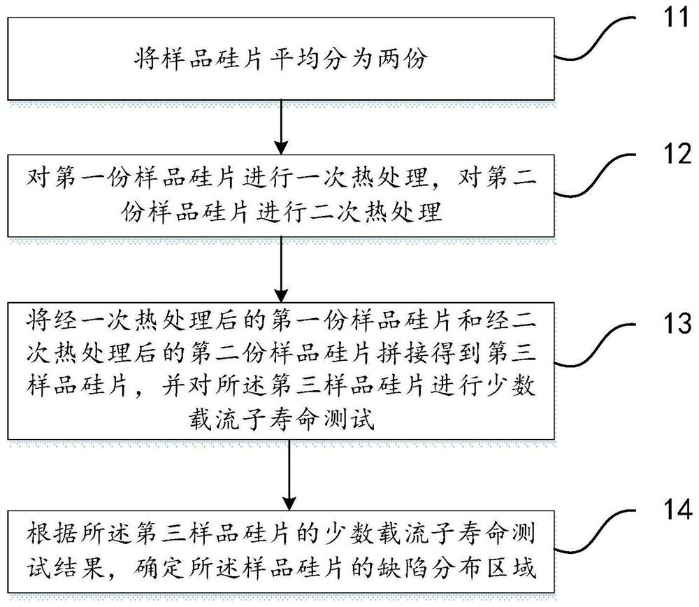
[0030] In order to make the purpose, technical solutions and advantages of the embodiments of the present invention more clear, the following will clearly and completely describe the technical solutions of the embodiments of the present invention in conjunction with the drawings of the embodiments of the present invention. Apparently, the described embodiments are some, not all, embodiments of the present invention. All other embodiments obtained by those skilled in the art based on the described embodiments of the present invention belong to the protection scope of the present invention.
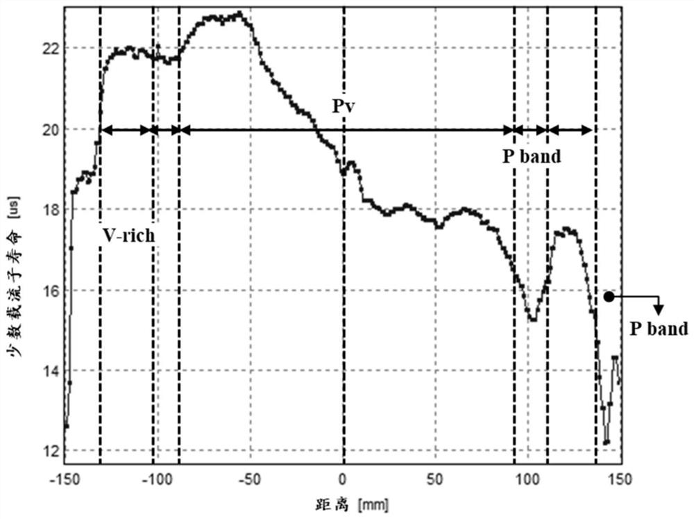
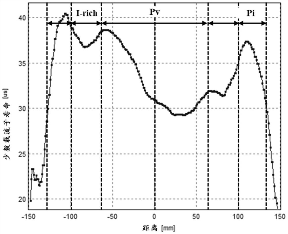
[0031] In order to determine the distribution area of different defects produced in the growth process of single crystal silicon, the methods adopted are as follows: first, clean the polished silicon wafer, and then use a particle counter to count and evaluate; second The first is to use corrosive liquid for etching (Secco etching), and then evaluate the fluid pattern defect FPD (Flow Pat...
PUM
 Abstract
Description
Claims
Application Information
 - R&D Engineer
- R&D Manager
- IP Professional
- Industry Leading Data Capabilities
- Powerful AI technology
- Patent DNA Extraction
Browse by: Latest US Patents, China's latest patents, Technical Efficacy Thesaurus, Application Domain, Technology Topic.
© 2024 PatSnap. All rights reserved.Legal|Privacy policy|Modern Slavery Act Transparency Statement|Sitemap