Array substrate and manufacturing method thereof

A technology of an array substrate and a manufacturing method, which is applied in the field of display panels, can solve problems such as film layer breakage, achieve the effects of reducing area, preventing electrode layer breakage, and reducing lap resistance

Pending Publication Date: 2020-09-01
NANJING CEC PANDA LCD TECH
View PDF7 Cites 0 Cited by
  • Summary
  • Abstract
  • Description
  • Claims
  • Application Information

AI Technical Summary

Problems solved by technology

Compared with the conventional terminal area film design, this design occupies a smaller area, can reduce the panel frame and increase the aperture ratio, but the gate insulating layer (GI) under the signal electrode layer will have over-etched areas, and over-etched There is a tendency to cause subsequent film layers to break during the manufacturing process

Method used


Image

  • Array substrate and manufacturing method thereof
  • Array substrate and manufacturing method thereof
  • Array substrate and manufacturing method thereof

Examples


Embodiment Construction

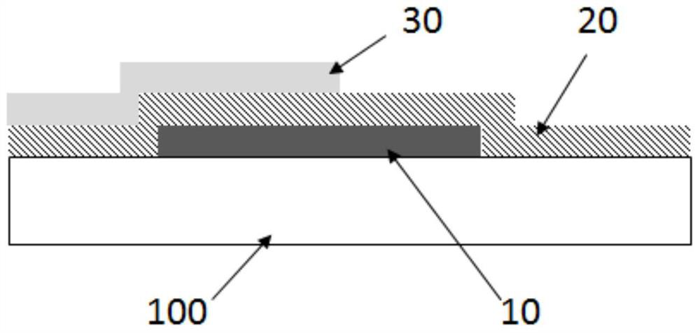
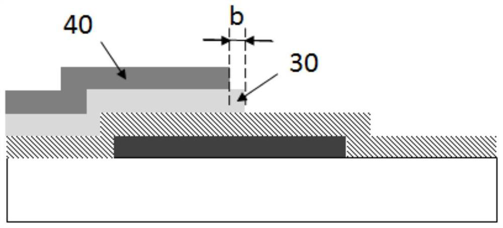
[0032] In order to more clearly illustrate the embodiments of the present invention or the technical solutions in the prior art, the specific implementation manners of the present invention will be described below with reference to the accompanying drawings. Obviously, the accompanying drawings in the following description are only some embodiments of the present invention, and those skilled in the art can obtain other accompanying drawings based on these drawings and obtain other implementations.

[0033] In order to make the drawing concise, each drawing only schematically shows the parts related to the present invention, and they do not represent the actual structure of the product. In addition, to make the drawings concise and easy to understand, in some drawings, only one of the components having the same structure or function is schematically shown, or only one of them is marked. Herein, "a" not only means "only one", but also means "more than one".

[0034] The techni...


PUM

PropertyMeasurementUnit
widthaaaaaaaaaa

Abstract

The invention provides an array substrate and a manufacturing method thereof, and relates to the field of display panels. The manufacturing method of the array substrate comprises the steps of S1, forming a gate metal layer, a gate insulating layer covering the gate metal layer, and a semiconductor layer located on the gate insulating layer on a substrate; S2, forming a signal electrode layer located on the semiconductor layer, wherein part of the semiconductor layer is covered with the signal electrode layer, and the semiconductor layer is provided with an edge part exposed out of the signalelectrode layer; S3, sequentially depositing an inorganic insulating layer and a light resistor on the basis of the step S2, forming a first opening hole located on the gate metal layer and a second opening hole communicated with the first opening hole through exposure etching, wherein the second opening hole exposes the edge part of the semiconductor layer; S4, etching the edge part of the semiconductor layer exposed out of the lower layer of the exposed signal electrode layer; and S5, stripping a photoresist to form a transparent electrode layer located in the first open pore and the secondopen pore.

Description

technical field [0001] The invention belongs to the field of display panels, and in particular relates to an array substrate and a manufacturing method thereof. [0002] technical background [0003] In the field of liquid crystal display technology, the manufacture of array substrates is a key link. In the prior art, for the terminal area on the array substrate, a part of the signal electrode layer (SD) is superimposed on the gate metal layer (Gate), and then a hole is opened in the inorganic insulating layer (PAS), and the transparent electrode layer is used to cover the terminal area. The signal electrode layer and the gate metal layer are connected. Compared with the conventional terminal area film design, this design occupies a smaller area, can reduce the panel frame, and increase the aperture ratio, but the gate insulating layer (GI) under the signal electrode layer will have over-etched areas, and over-etched It is easy to cause subsequent film layers to break durin...

Claims


Application Information

Patent Timeline
Patent Type & Authority Applications(China)
IPC IPC(8): H01L21/77H01L27/12G02F1/1362
CPCH01L27/1288H01L27/1225H01L27/1244G02F1/136227
Inventor 易志根潘明超殷大山
Owner NANJING CEC PANDA LCD TECH
Why Eureka
Try Eureka