


Quick Research
Generate reliable direction feasibility study reports for your R&D in just a few steps.

Technical Q&A
Discover and master advanced knowledge NOW. Basics, ideas, possibilities, all at once.

Find Solutions
As an expert in R&D theories, this can generate solutions to your technical problems instantly.

Evaluate Feasibility
Analyze your overall solution with one click, know your potential R&D risks in advance.

Monitor Landscape
Get weekly tech updates, stay abreast of the latest tech innovations and key insights.
Electron microscope in-situ sample rod with high-resolution multidimensional manipulation and electrical measurement
An electron microscope, high-resolution technology, used in circuits, discharge tubes, electrical components, etc., can solve the problems of inability to meet the needs of high-resolution electron microscopes and limited resolution
- Summary
- Abstract
- Description
- Claims
- Application Information
AI Technical Summary
Problems solved by technology
Method used
Image

Examples
Embodiment 1
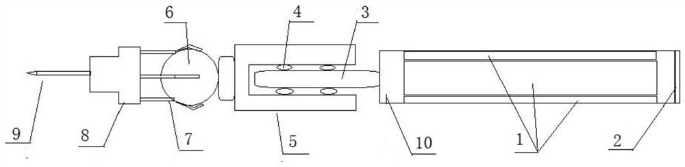
[0039] Such as figure 1 As shown, the present invention discloses an in-situ micro area manipulation and physical property measurement scheme based on piezoelectric ceramics and inertial sensing for modern high-resolution electron microscopes.
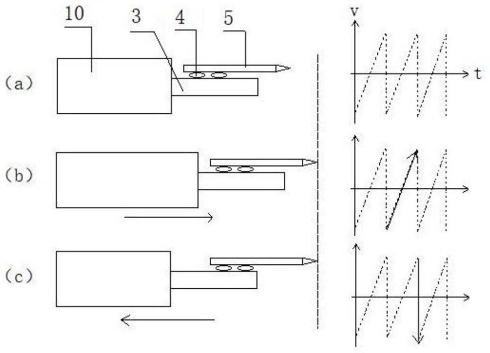
[0040] The in-situ sample rod 11 of the electron microscope with high-resolution multi-dimensional manipulation and electrical measurement. The end of the sample rod 11 is provided with a rod head body. The rod head body includes a micro-manipulation structure and a probe 9. The manipulation structure is provided with a deformation mechanism and a telescopic mechanism. Mechanism, the deformation mechanism is connected with the probe 9 through the telescopic mechanism;
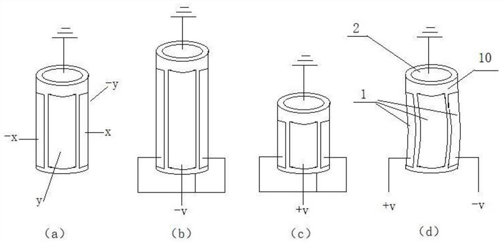
[0041] The deformation mechanism includes a piezoelectric ceramic sheet group 1 and a base base 10. The base base 10 is made of a non-conductive material to form a hollow cylindrical structure, which has the characteristics of being hollow, non-conductive, suitable for toughn...
Embodiment 2
[0047] Such as figure 1 As shown, on the basis of embodiment 1, it is different from embodiment 1, as figure 1 , Figure 5 with Image 6 As shown, the electron microscope in-situ sample rod 11 with high-resolution multi-dimensional manipulation and electrical measurement is provided with a rod head body at the end of the sample rod 11, and the rod head body includes a micro-manipulation structure and a probe 9, and the manipulation structure is provided with deformation Mechanism, telescopic mechanism and inertial sensing mechanism, the deformation mechanism is connected with the probe 9 through the telescopic mechanism;
[0048] The inertial sensing mechanism is arranged in a spherical gravity block structure, and the spherical gravity block is firmly connected to the outer end of the slider.
[0049] The inertial sensing mechanism is sequentially provided with a copper cap 8, a metal claw 7 and a gravity ball 6. The probe 9 is connected to the copper cap 8 in a detachable manner,...
Embodiment 3
[0055] On the basis of embodiment 1 or 2, different from embodiment 1 or 2, such as figure 1 , Figure 5 with Image 6 As shown, the in-situ sample rod 11 of the electron microscope with high-resolution multi-dimensional manipulation and electrical measurement is provided with an outer frame 13 on the outside of the head body and installed at the end of the sample rod 11 through the outer frame 13. The outer frame 13 and the head The probe 9 of the body is correspondingly provided with a sample loading area, such as Figure 5 As shown, the sample loading area is facing the micro-manipulation structure. The loading area can be a conductive needle or a semi-copper mesh structure. This depends on whether the selected sample is a nanowire, a nanoparticle, or a block or film. A circuit structure is printed on the outer frame 13, one end of the circuit is electrically connected to the sample area 12, and the other end of the circuit passes through the shaft of the sample rod 11 throug...
PUM
 Abstract
Description
Claims
Application Information
 - R&D Engineer
- R&D Manager
- IP Professional
- Industry Leading Data Capabilities
- Powerful AI technology
- Patent DNA Extraction
Browse by: Latest US Patents, China's latest patents, Technical Efficacy Thesaurus, Application Domain, Technology Topic, Popular Technical Reports.
© 2024 PatSnap. All rights reserved.Legal|Privacy policy|Modern Slavery Act Transparency Statement|Sitemap|About US| Contact US: help@patsnap.com