Touch display device

A touch display device, touch layer technology, applied in the direction of instrument, electrical digital data processing, data processing input/output process, etc., can solve problems such as poor touch operation experience, reduce parasitic capacitance, improve touch The effect of the reporting rate

Active Publication Date: 2020-08-28
WUHAN CHINA STAR OPTOELECTRONICS SEMICON DISPLAY TECH CO LTD
View PDF9 Cites 3 Cited by
  • Summary
  • Abstract
  • Description
  • Claims
  • Application Information

AI Technical Summary

Problems solved by technology

For capacitive touch screens, the higher the touch report rate, the smoother the user's touch operation, on the contrary, the lower the touch report rate, the worse the touch operation experience

Method used


Image

  • Touch display device
  • Touch display device
  • Touch display device

Examples


no. 1 example

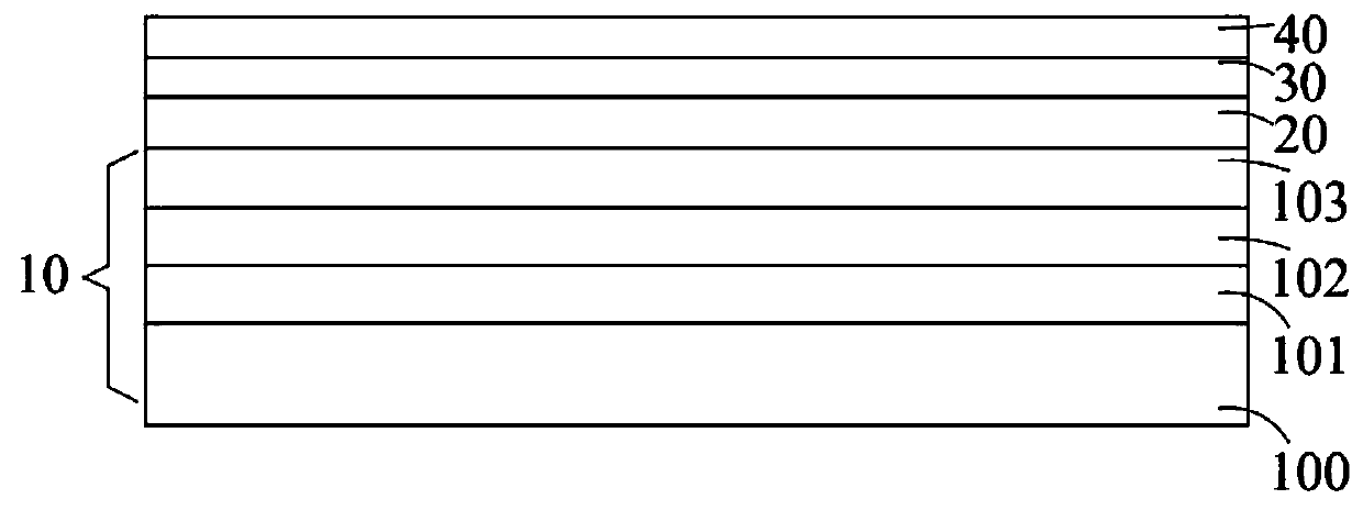
[0077] see figure 1 , which is a schematic diagram of the touch display device of the present application. The touch display device includes an OLED display panel 10 , a touch layer 20 , a polarizer 30 and a protective cover 40 .

[0078] The OLED display panel 10 includes a substrate 100 , a TFT array layer 101 , an OLED array layer 102 and an encapsulation layer 103 .

[0079]The substrate 100 is a flexible substrate. The thin film transistor array layer 101 is disposed on the substrate 100, and the thin film transistor array layer 101 includes a plurality of thin film transistors arranged in an array. The OLED array layer 102 is disposed on a side of the TFT array layer 101 away from the substrate 100 . The organic light emitting diode array layer 102 includes a plurality of organic light emitting diodes arranged in an array, and the plurality of organic light emitting diodes includes a plurality of independent anodes, an organic light emitting layer disposed on each ano...

no. 2 example and comparative example 1

[0088] The following combines the touch units of the embodiment and the comparative example to study the influence of the metal area of ​​the touch unit on the 3RC time constant, mutual capacitance, and capacitance variation, and to study the relationship between the metal area of ​​the driving electrode, the sensing electrode, and the floating electrode The effect of the proportion of the total metal area on the 3RC time constant, mutual capacitance and capacitance variation. Among them, the capacitance change mainly affects the touch sensitivity, the parasitic capacitance affects the 3RC time constant, and the 3RC time constant mainly affects the touch report rate.

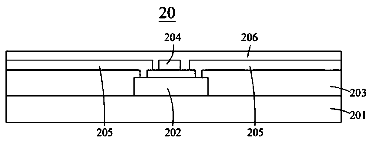
[0089] like Figure 5A As shown, it is a schematic diagram of the touch unit 1 of the present application. The touch unit 1 includes a driving electrode 204 , a sensing electrode 205 and a floating electrode 210 . The driving electrode 204 includes a first main electrode 2041 extending in a first direction and...


PUM

PropertyMeasurementUnit
lengthaaaaaaaaaa
widthaaaaaaaaaa
widthaaaaaaaaaa

Abstract

The invention provides a touch display device. The touch display device comprises an organic light-emitting diode display panel and a touch assembly, the organic light-emitting diode display panel comprises a common cathode and a packaging layer, the touch control assembly comprises a touch control layer, the packaging layer is located between the common cathode and the touch control layer, the touch control layer comprises a plurality of touch control units arranged in an array mode, each touch control unit is composed of metal grids, and in each touch control unit, the percentage of the ratio of the metal area of the metal grids to the area of each touch control unit is larger than 0% and smaller than or equal to 25%. The metal area ratio of the metal grid in each touch unit is optimizedto reduce the parasitic capacitance between each touch unit and the common cathode, so that the touch reporting rate of the touch display device is improved.

Description

technical field [0001] The present application relates to the field of touch technology, in particular to a touch display device. Background technique [0002] Capacitive touch screens are widely used in various electronic interactive scene devices due to their high durability and long life, and support for multi-touch functions. For a capacitive touch screen, the higher the touch report rate, the smoother the user's touch operation, and on the contrary, the lower the touch report rate, the worse the touch operation experience. [0003] Therefore, it is necessary to provide a technical solution to improve the touch reporting rate of the touch display device. Contents of the invention [0004] The purpose of the present application is to provide a touch display device to improve the touch reporting rate of the touch display device. [0005] In order to achieve the above purpose, the present application provides a touch display device, the touch display device includes an ...

Claims


Application Information

Patent Timeline
Patent Type & Authority Applications(China)
IPC IPC(8): G06F3/041G06F3/044
CPCG06F3/0412G06F3/0446G06F2203/04112H10K59/873G06F3/0448H10K59/40G06F3/04166G06F3/0443H10K50/844
Inventor 叶剑
Owner WUHAN CHINA STAR OPTOELECTRONICS SEMICON DISPLAY TECH CO LTD
Why Eureka
Try Eureka