Optical system, receiving module and electronic equipment
An optical system and module technology, applied in the field of three-dimensional imaging, can solve the problems that TOF three-dimensional imaging devices cannot meet the miniaturization design of electronic equipment, etc.
- Summary
- Abstract
- Description
- Claims
- Application Information
AI Technical Summary
Problems solved by technology
Method used
Image
Examples
no. 1 example
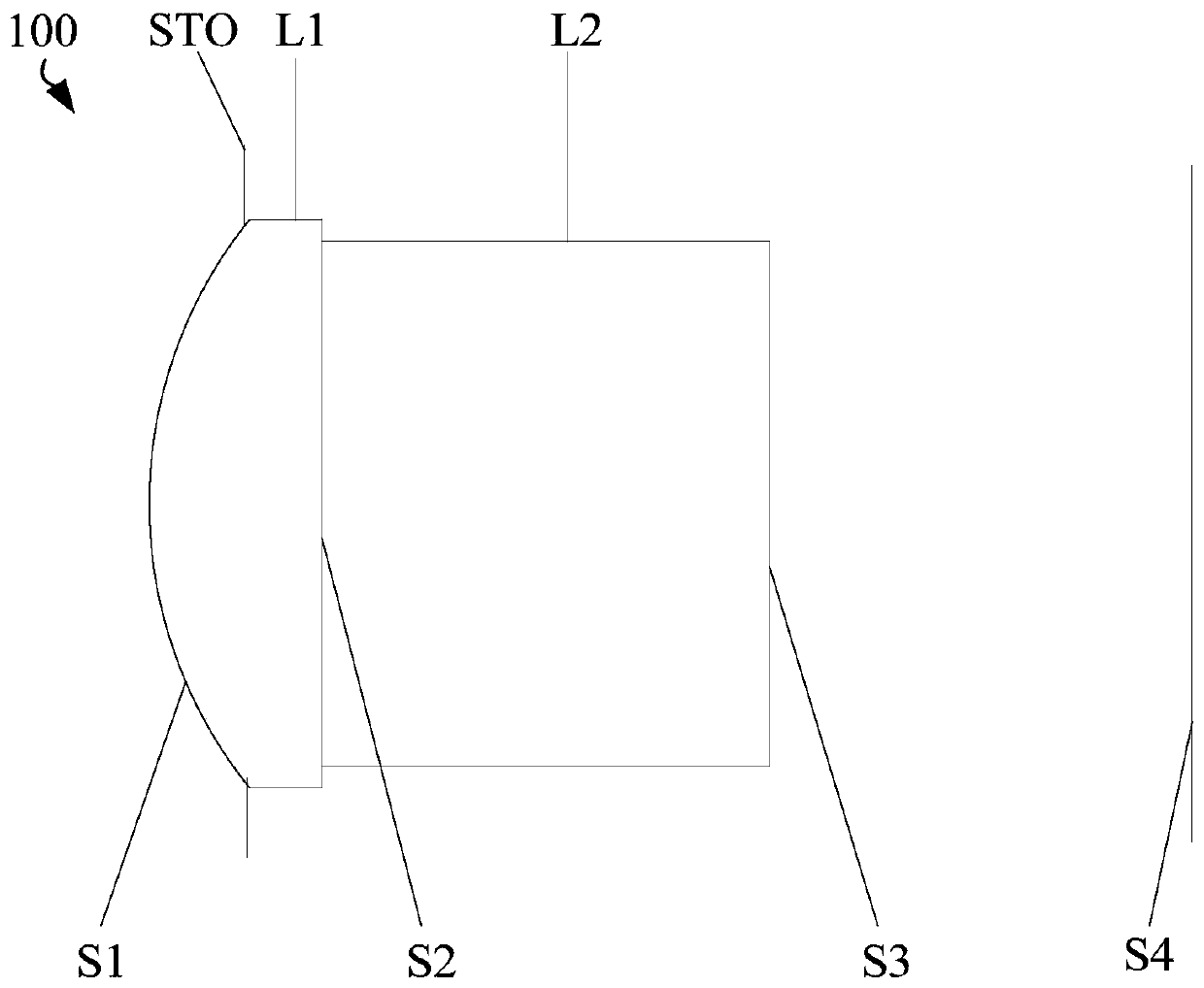
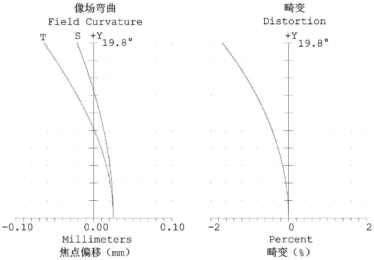
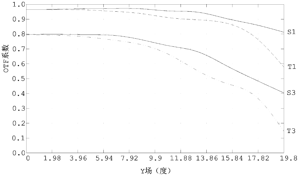
[0057] See figure 1 , figure 2 with image 3 , figure 1 It is a schematic diagram of the optical system 100 in the first embodiment. The optical system 100 includes a stop STO, a lens L1 with a positive refractive power, and an infrared band pass filter L2 in order from the object side to the image side.
[0058] The diaphragm STO is provided on the object side S1 of the lens L1. Specifically, the diaphragm STO can be formed by attaching a lens frame and a light barrier to the object side S1 of the lens L1. The object side surface S1 of the lens L1 is convex and aspherical. The lens L1 is formed on the object side of the infrared band pass filter L2 by embossing. The image side surface S2 of the lens L1 is a plane, that is, the image side surface S2 of the lens L1 can be regarded as a spherical surface with an infinite radius of curvature. Both the object side and the image side S3 of the infrared band pass filter L2 are flat surfaces. The image plane S4 is spaced apart from t...
no. 2 example
[0077] See Figure 4 , Figure 5 with Image 6 , Figure 4 It is a schematic diagram of the optical system 100 in the second embodiment. The optical system 100 includes a stop STO, a lens L1 with a positive refractive power, and an infrared band pass filter L2 in order from the object side to the image side.
[0078] The stop STO is provided on the object side of the lens L1 and is spaced apart from the lens L1. Specifically, the stop STO can be formed by fixing a lens frame or a light blocking plate to the object side of the lens L1. The object side surface S1 of the lens L1 is convex and aspherical. The lens L1 is formed on the object side of the infrared bandpass filter L2 by embossing. The image side surface S2 of the lens L1 is a plane, that is, the image side surface S2 of the lens L1 can be regarded as a spherical surface with an infinite radius of curvature. Both the object side and the image side S3 of the infrared bandpass filter L2 are flat surfaces. The image surfac...
no. 3 example
[0090] See Figure 7 , Picture 8 with Picture 9 , Figure 7 It is a schematic diagram of the optical system 100 in the third embodiment. The optical system 100 includes a lens L1 having a positive refractive power, a stop STO, and an infrared band pass filter L2 in order from the object side to the image side.
[0091] The diaphragm STO is arranged on the image side surface S2 of the lens L1, and the lens L1 includes a lens portion 110 and a coupling portion 120. The diaphragm STO is formed by a light shield surrounding the coupling portion 120. Specifically, refer to Figure 7 As shown, first, a layer of light shield 130 is provided on the object side of the infrared band pass filter L2, wherein the middle part of the light shield 130 transmits light. Then, the UV glue for manufacturing the lens L1 is stamped on the object side of the light shield 130, and a part of the UV glue is filled in the middle part of the light shield 130. Furthermore, ultraviolet light is used to cure...
PUM
| Property | Measurement | Unit |
|---|---|---|
| Wavelength | aaaaa | aaaaa |
Abstract
Description
Claims
Application Information
 - R&D
- Intellectual Property
- Life Sciences
- Materials
- Tech Scout
- Unparalleled Data Quality
- Higher Quality Content
- 60% Fewer Hallucinations
Browse by: Latest US Patents, China's latest patents, Technical Efficacy Thesaurus, Application Domain, Technology Topic, Popular Technical Reports.
© 2025 PatSnap. All rights reserved.Legal|Privacy policy|Modern Slavery Act Transparency Statement|Sitemap|About US| Contact US: help@patsnap.com


