DC-AC converter switching-period-by-switching-period peak current limiting system and method
A technology of DC-AC and peak current, which is applied in the field of peak current limiting system of DC-AC converter by switching cycle, which can solve the problems such as difficult to realize peak current limiting, so as to improve system reliability, fast response speed, eliminate Effects of Subharmonic Oscillations
- Summary
- Abstract
- Description
- Claims
- Application Information
AI Technical Summary
Problems solved by technology
Method used
Image
Examples
Embodiment 1
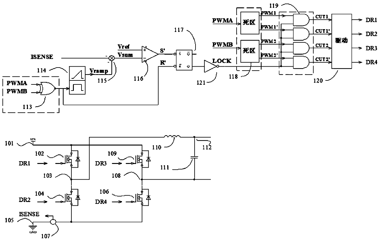
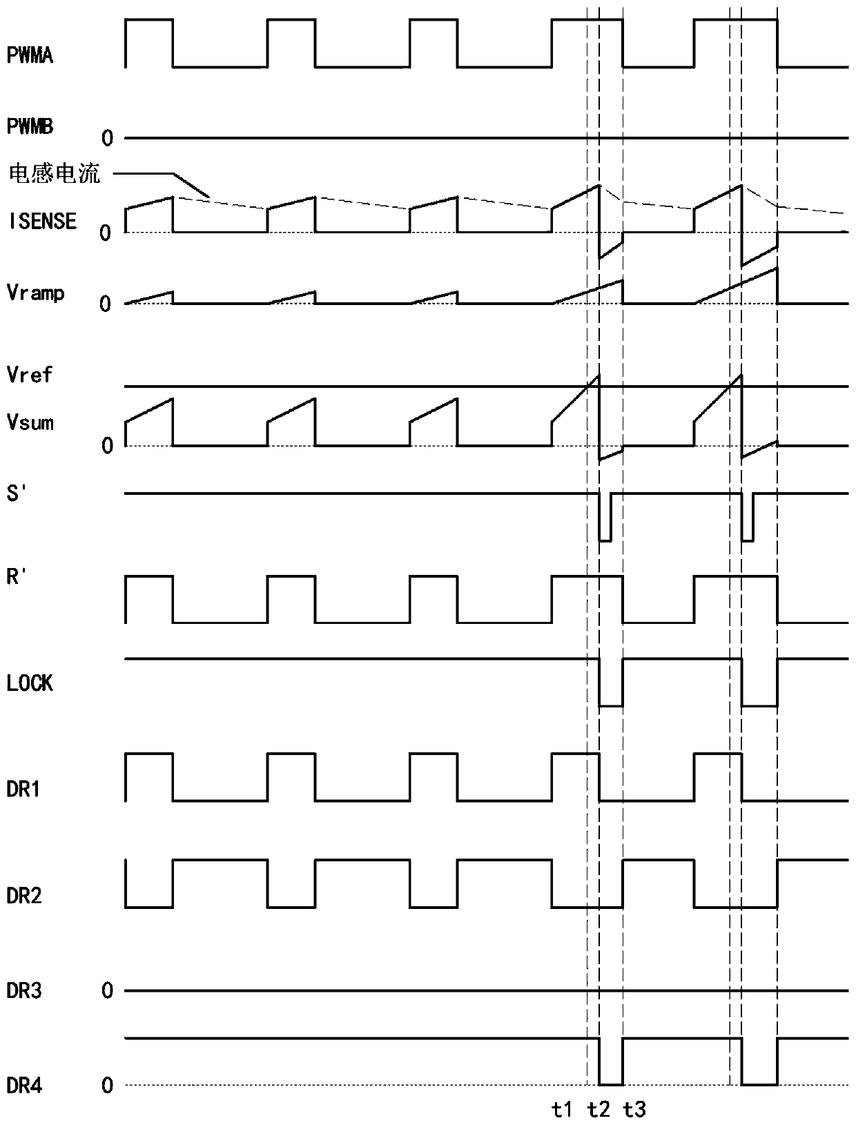
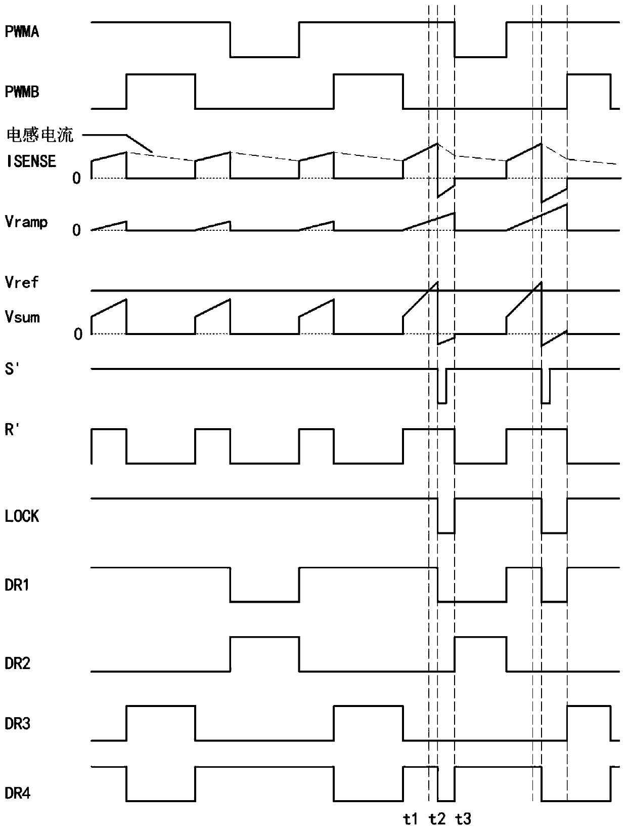
[0086] figure 1 A schematic diagram of the switching cycle-by-switching peak current limiting system of the DC-AC converter according to the embodiment of the present invention is given. The power execution part and the current limiting control part of the DC-AC converter are mainly described below.
[0087] In the H-bridge circuit of the DC-AC converter, the input voltage 101 is applied to the drains of the first switch transistor 102 and the third switch transistor 109, and the input ground 105 is connected to the second switch transistor 104 and the fourth switch through the current sensor 107. The source of the transistor 106, the source of the first switching transistor 102 and the drain of the second switching transistor 104 and one end of the inductor 110 are connected to the first voltage node 103, the source of the third switching transistor 109 and the fourth switching transistor The drain of the inductor 106 and one end of the capacitor 111 are connected to the sec...
Embodiment 2
[0102] In Embodiment 1, the current sampling point is located in the DC input loop, that is, the current sensor collects the DC input current of the H-bridge, and the sensor will introduce parasitic inductance, which has an adverse effect on the switching transistor, and is not suitable for DC-AC conversion with a power greater than 10kW device, while this example gives Figure 5 The inductor current sampling method shown can be used for DC-AC converters exceeding 10kW. The difference between this embodiment and the first embodiment is that the sampling position of the current sensor 107 is different, and the current sensing signal ISENSE is generated after passing through the rectification circuit 122 . Figure 5 The medium current sensor 107 adopts a Hall sensor and is located between the inductor 110 and the first voltage node 103 . The output signal of the current sensor 107 passes through the rectification circuit 122 to generate a current sensing signal ISENSE. The work...
PUM
 Abstract
Description
Claims
Application Information
 - R&D Engineer
- R&D Manager
- IP Professional
- Industry Leading Data Capabilities
- Powerful AI technology
- Patent DNA Extraction
Browse by: Latest US Patents, China's latest patents, Technical Efficacy Thesaurus, Application Domain, Technology Topic, Popular Technical Reports.
© 2024 PatSnap. All rights reserved.Legal|Privacy policy|Modern Slavery Act Transparency Statement|Sitemap|About US| Contact US: help@patsnap.com


