
Fan-out type packaging structure and packaging method

A packaging structure, fan-out technology, applied in electrical components, electrical solid devices, circuits, etc., can solve the problems of easy mutual interference, defective chips, and inability to shield chip electromagnetic interference.

Active Publication Date: 2020-08-21
FOREHOPE ELECTRONICS NINGBO CO LTD
View PDF4 Cites 0 Cited by
  • Summary
  • Abstract
  • Description
  • Claims
  • Application Information

AI Technical Summary

Problems solved by technology

[0004] However, during the use of the current fan-out double-sided packaging structure, the electromagnetic interference generated between the internal chips cannot be shielded, which leads to the mutual interference between the chips and causes defects, which reduces the performance of the packaged product.

Method used


Image

  • Fan-out type packaging structure and packaging method
  • Fan-out type packaging structure and packaging method
  • Fan-out type packaging structure and packaging method

Examples


Embodiment Construction

[0037] In order to make the purpose, technical solutions and advantages of the embodiments of the present invention clearer, the technical solutions in the embodiments of the present invention will be clearly and completely described below in conjunction with the drawings in the embodiments of the present invention. Obviously, the described embodiments It is a part of embodiments of the present invention, but not all embodiments. The components of the embodiments of the invention generally described and illustrated in the figures herein may be arranged and designed in a variety of different configurations.

[0038] Accordingly, the following detailed description of the embodiments of the invention provided in the accompanying drawings is not intended to limit the scope of the claimed invention, but merely represents selected embodiments of the invention. Based on the embodiments of the present invention, all other embodiments obtained by persons of ordinary skill in the art wi...


PUM


Abstract

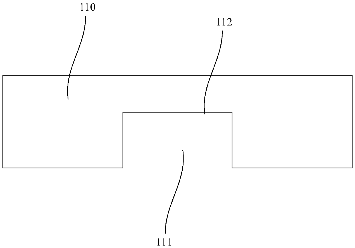
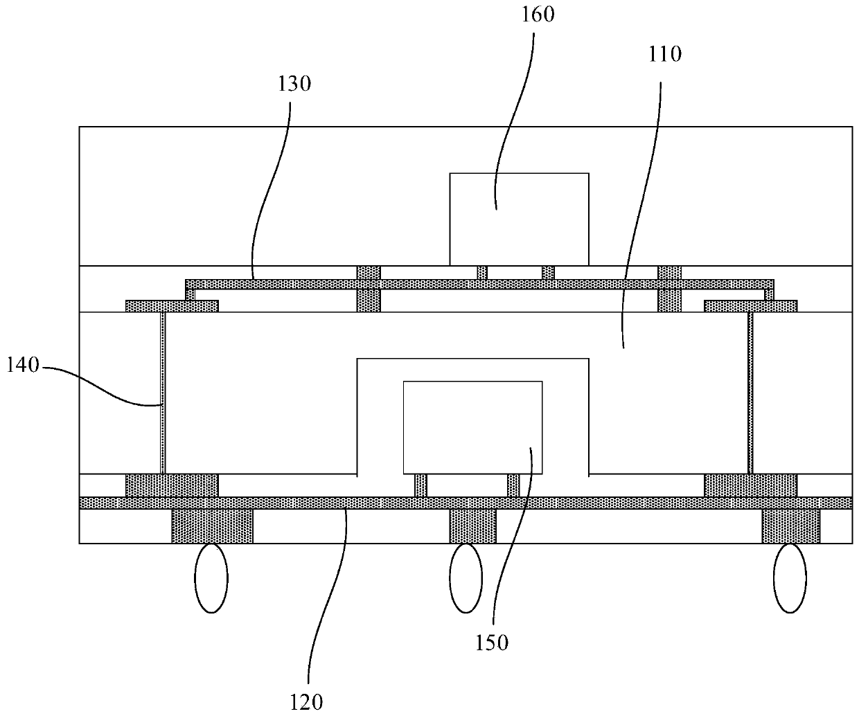
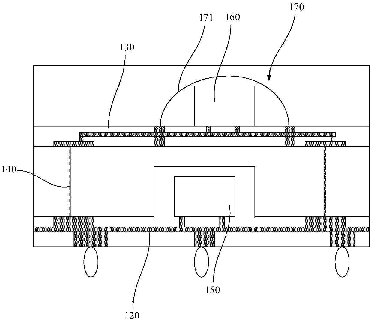
The invention provides a fan-out type packaging structure and a fan-out type packaging method, and belongs to the technical field of chip packaging. The fan-out type packaging structure comprises a plate-shaped base material, an accommodating groove is formed in a plate surface at one side of the plate-shaped base material, a first rewiring layer and a second rewiring layer are respectively formedon two side plate surfaces of the plate-shaped base material; the first rewiring layer and the second rewiring layer are connected through a conductive column. The conductive columns penetrate through the plate-shaped base material; a first chip is accommodated in the accommodating groove; a circuit bonding pad of the first chip is located at the side far away from the bottom of the accommodatinggroove and is connected with the first rewiring layer; a first shielding body is arranged in the accommodating groove, the periphery of the first chip is covered with the first shielding body, the side, away from the plate-shaped base material, of the second rewiring layer is connected with a second chip, a second shielding body is formed on the second rewiring layer, and the periphery of the second chip is covered with the second shielding body. The packaging structure can shield electromagnetic interference between chips so as to avoid badness caused by mutual interference between the chipsand improve the product performance of the packaging structure.

Description

technical field [0001] The present invention relates to the technical field of chip packaging, in particular to a fan-out packaging structure and packaging method. Background technique [0002] With the rapid development of the semiconductor industry, a Fan-out wafer level package (FOWLP) structure is widely used in the semiconductor industry. [0003] Among them, when packaging multiple chips, chips with different functions are generally packaged on both sides to achieve high-density integration, reduce the size of packaged products, improve product performance, and speed up signal transmission frequency. [0004] However, during the use of the current fan-out double-sided packaging structure, the electromagnetic interference generated between the internal chips cannot be shielded, which will easily cause mutual interference between the chips and cause defects, and reduce the performance of the packaged product. Contents of the invention [0005] The purpose of the prese...

Claims


Application Information

Patent Timeline
IPC IPC(8): H01L25/18H01L23/552H01L23/31H01L21/56H01L23/485H01L21/60
CPCH01L25/18H01L23/3128H01L23/552H01L24/02H01L24/03H01L21/56H01L2224/02331H01L2224/02381H01L2224/02379H01L2224/031H01L2224/16225H01L2924/19107
Inventor 王顺波
Owner FOREHOPE ELECTRONICS NINGBO CO LTD
Learn More