Semiconductor device and manufacturing method thereof

A manufacturing method and semiconductor technology, applied in semiconductor/solid-state device manufacturing, electrical components, circuits, etc., can solve problems affecting process and device reliability, and achieve the effect of improving reliability and uniformity

Inactive Publication Date: 2020-08-21
YANGTZE MEMORY TECH CO LTD
View PDF5 Cites 4 Cited by
  • Summary
  • Abstract
  • Description
  • Claims
  • Application Information

AI Technical Summary

Problems solved by technology

[0003] After wafer bonding, the substrate of the upper wafer needs to be thinned. The total thickness variation (Total Thickness Variation, TTV) of the substrate surface after thinning is relatively large, which affects the subsequent process and further affects the device. reliability

Method used


Image

  • Semiconductor device and manufacturing method thereof
  • Semiconductor device and manufacturing method thereof
  • Semiconductor device and manufacturing method thereof

Examples


Embodiment Construction

[0043] In order to make the above objects, features and advantages of the present invention more comprehensible, specific implementations of the present invention will be described in detail below in conjunction with the accompanying drawings.

[0044] In the following description, a lot of specific details are set forth in order to fully understand the present invention, but the present invention can also be implemented in other ways different from those described here, and those skilled in the art can do it without departing from the meaning of the present invention. By analogy, the present invention is therefore not limited to the specific examples disclosed below.

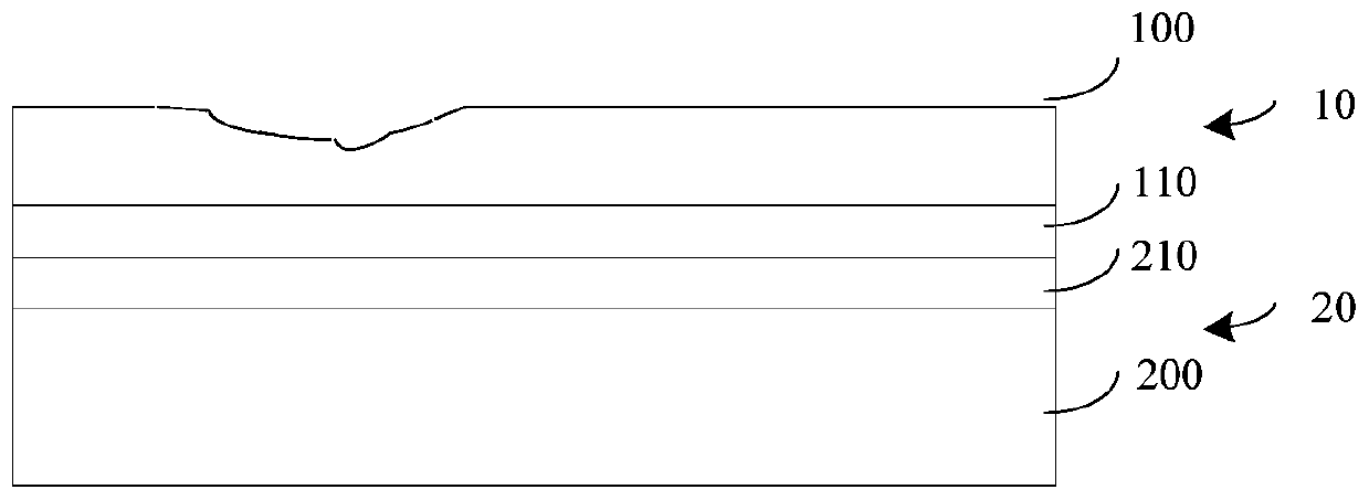
[0045] As described in the background art, refer to figure 1 As shown, the first wafer 10 and the second wafer 20 are bonded through the first dielectric bonding layer 110 and the second dielectric bonding layer 210. After the first wafer 10 and the second wafer 20 are bonded, The first substrate 100 of the fi...


PUM

PropertyMeasurementUnit
thicknessaaaaaaaaaa

Abstract

The invention provides a semiconductor device and a manufacturing method thereof, and provides a wafer bonding structure, which comprises a first wafer and a second wafer which are bonded, wherein thefirst wafer comprises a first substrate and a first dielectric layer, the surface of the first dielectric layer is used as a bonding surface of the first wafer and the second wafer, a barrier layer is formed in the first substrate, and by using the barrier layer as an etching stop layer, the first substrate is thinned from the surface of the first substrate so as to remove the first substrate material above the barrier layer in the process of thinning the first wafer without damaging the barrier layer, so that the uniformity of the surface of the thinned first substrate is improved, and the subsequent process is facilitated so as to further improve the reliability of the device.

Description

technical field [0001] The invention relates to the field of semiconductor integrated circuit manufacturing, in particular to a semiconductor device and a manufacturing method thereof. Background technique [0002] With the continuous development of semiconductor technology, bonding packaging technology has been widely used, which uses bonding technology to stack and bond different devices together. [0003] After wafer bonding, the substrate of the upper wafer needs to be thinned. The total thickness variation (Total Thickness Variation, TTV) of the substrate surface after thinning is relatively large, which affects the subsequent process and further affects the device. reliability. Contents of the invention [0004] In view of this, the object of the present invention is to provide a semiconductor device and a manufacturing method thereof, so as to improve the reliability of the device. [0005] To achieve the above object, the present invention has the following techn...

Claims


Application Information

Patent Timeline
Patent Type & Authority Applications(China)
IPC IPC(8): H01L21/306
CPCH01L21/30604H01L21/30625
Inventor 杨俊铖
Owner YANGTZE MEMORY TECH CO LTD
Why Eureka
Try Eureka