Data Relay Architecture for Configuration Memory of Programmable Logic Devices

A technology of data relay and programming logic, applied in static memory, digital memory information, information storage, etc., can solve problems such as the inability to meet the large-scale design of users, lack of data relay transmission and enhancement, and limited number of configuration memory levels. , to reduce voltage loss, reduce power consumption, and achieve flexible effects

Active Publication Date: 2022-02-18
WUXI ESIONTECH CO LTD +1
View PDF7 Cites 0 Cited by
  • Summary
  • Abstract
  • Description
  • Claims
  • Application Information

AI Technical Summary

Problems solved by technology

The number of common configuration memory series is limited, and the lack of data relay to transfer and strengthen data cannot meet the large-scale design requirements of users.

Method used


Image

  • Data Relay Architecture for Configuration Memory of Programmable Logic Devices
  • Data Relay Architecture for Configuration Memory of Programmable Logic Devices
  • Data Relay Architecture for Configuration Memory of Programmable Logic Devices

Examples


Embodiment Construction

[0019] The specific embodiments of the present invention will be further described below in conjunction with the accompanying drawings.

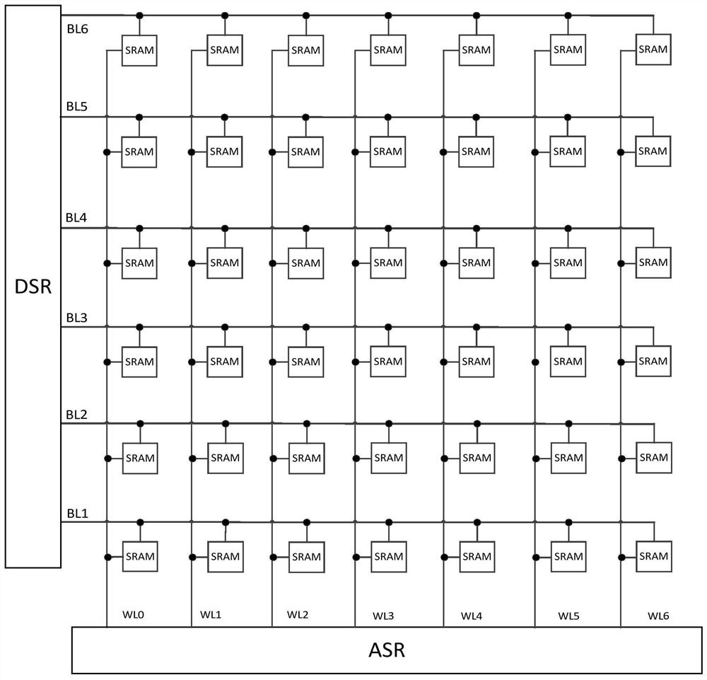
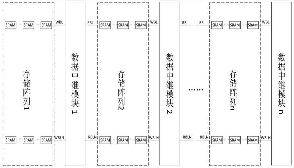
[0020] This application discloses a data relay structure for the configuration memory of programmable logic devices. The data relay structure includes cascading of several distributed data relay modules. When applying, please refer to figure 2 The configuration architecture of the data relay module and the storage array shown in the figure, n data relay modules and n storage arrays are cascaded to form the configuration architecture, each storage array contains multiple storage units SRAM, and the storage unit SRAM is a 6-pipe storage The cell contains two cross-coupled inverters, a write transistor and a read transistor. In the storage array, the data bit lines BL and BLN are connected to the storage unit SRAM.

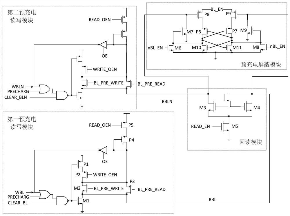
[0021] The data relay module of this application completes data transmission and data clearing, and the structure of each level...


PUM


Abstract

The invention discloses a data relay structure for a configuration memory of a programmable logic device, and relates to the technical field of programmable logic devices. The data relay structure includes cascading of several distributed data relay modules, and each data The relay module is composed of the pre-charged read-write module, the read-back module and the pre-charged shielding module with an enable terminal as the core. It does not occupy additional register units and is flexible. It can realize memory clearing, configuration data writing and configuration data return. Read three functions, and remove the pre-charge stage during the configuration data writing process, without charging RBL and RBLN to high level, thus reducing RBL voltage loss and programming power consumption, very suitable for ultra-large-scale programmable devices Configuration.

Description

technical field [0001] The invention relates to the technical field of programmable logic devices, in particular to a data relay structure for a configuration memory of a programmable logic device. Background technique [0002] Programmable logic device, based on the storage technology of repeated configuration, completes the modification of the circuit by re-downloading programming, has the advantages of short development cycle, low cost, low risk, and easy maintenance and upgrade of electronic systems, so it has become the mainstream of integrated circuit chips . Configuration memory is one of the most common functions in logic applications of programmable logic devices. Through configuration memory, the functions of data clearing / data configuration / data readback of the chip can be realized. [0003] Many complex integrated circuit chips need to load configuration information after the chip is reset, or reload specified configuration information in the working state. fig...

Claims


Application Information

Patent Timeline
Patent Type & Authority Patents(China)
IPC IPC(8): G11C7/10G11C7/22
CPCG11C7/10G11C7/22
Inventor 何小飞耿杨徐玉婷徐彦峰
Owner WUXI ESIONTECH CO LTD
Why Eureka
Try Eureka