Pixel circuit with voltage compensation function and driving method thereof and display panel

A pixel circuit and voltage compensation technology, applied in static indicators, instruments, etc., can solve the problems of complexity and multiple control signals of the pixel circuit, and achieve the effect of satisfying compatibility, small unit pixel area, and reducing the possibility of leakage

Inactive Publication Date: 2020-08-04
INST OF MICROELECTRONICS CHINESE ACAD OF SCI
View PDF8 Cites 0 Cited by
  • Summary
  • Abstract
  • Description
  • Claims
  • Application Information

AI Technical Summary

Problems solved by technology

[0005] What the present invention aims to solve is the problem that there are many and complex control signals of the existing pixel circuit that can be applied to the simultaneous light-emitting driving mode and has a voltage compensation function

Method used


Image

  • Pixel circuit with voltage compensation function and driving method thereof and display panel
  • Pixel circuit with voltage compensation function and driving method thereof and display panel
  • Pixel circuit with voltage compensation function and driving method thereof and display panel

Examples


Embodiment Construction

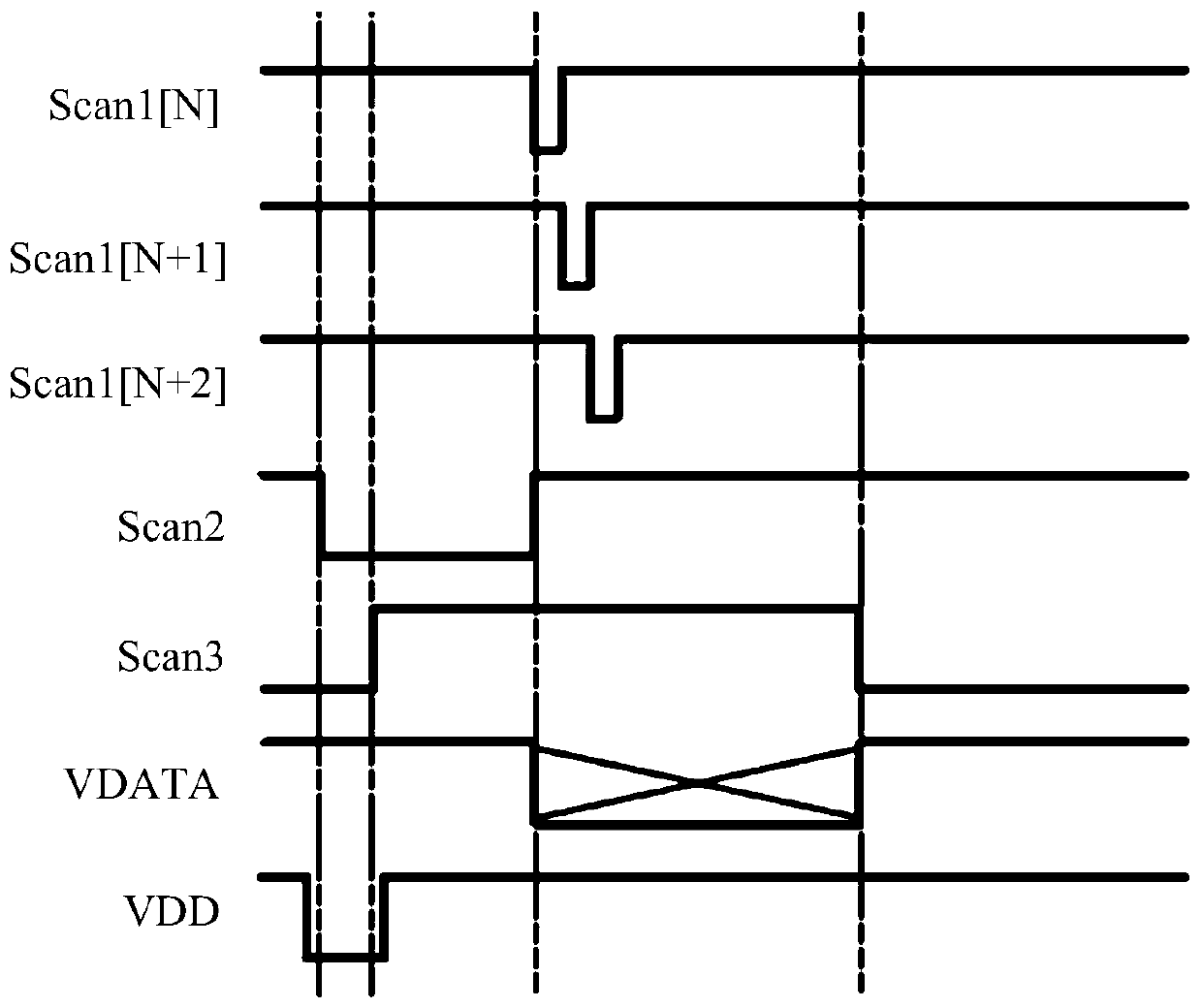
[0047] In order to make the purpose, technical solutions and advantages of the present invention clearer, the present invention will be further described in detail below in conjunction with the examples and accompanying drawings. As a limitation of the present invention.

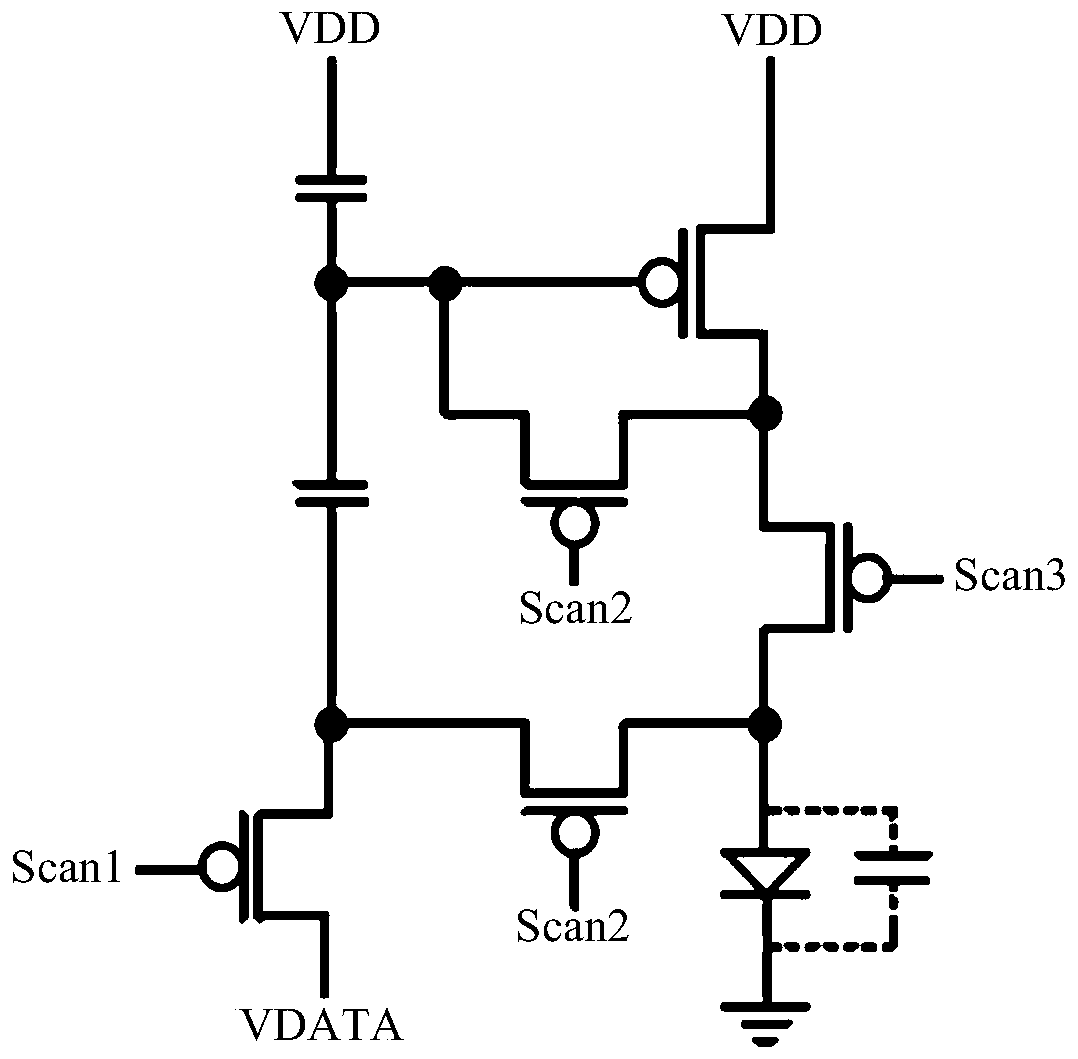
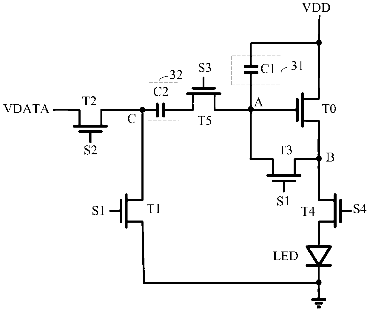
[0048] An embodiment of the present invention provides a pixel circuit with a voltage compensation function, image 3 It is a circuit diagram of the pixel circuit, and the pixel circuit includes a driving transistor T0, a first switching tube T1, a second switching tube T2, a third switching tube T3, a fourth switching tube T4, a fifth switching tube T5, and an energy storage unit 31. A coupling unit 32 and a light emitting diode LED.

[0049] One end of the driving transistor T0 is used to receive the power supply voltage VDD, and the control end of the driving transistor T0 is connected to the energy storage unit 31 , the other end of the fifth switching transistor T5 and one end of the third switching tr...


PUM


Abstract

The invention discloses a pixel circuit with a voltage compensation function and a driving method thereof and a display panel. The pixel circuit comprises a driving transistor, a first switching tube,a second switching tube, a third switching tube, a fourth switching tube, a fifth switching tube, an energy storage unit, a coupling unit and a light emitting diode. One end of the driving transistorreceives a power supply voltage, the control end of the driving transistor is connected with the energy storage unit, the other end of the fifth switching tube and one end of the third switching tube, and the other end of the driving transistor is connected with the other end of the third switching tube and one end of the fourth switching tube; one end of the second switch tube receives the datasignal, and the other end of the second switching tube is connected with one end of the coupling unit and one end of the first switching tube; the other end of the coupling unit is connected with oneend of a fifth switching tube; the other end of the fourth switching tube is connected with the anode of the light emitting diode; the cathode of the light emitting diode and the other end of the first switching tube are grounded. The pixel circuit provided by the invention meets the requirements of high resolution and narrow frame.

Description

technical field [0001] The invention relates to the technical field of display control, in particular to a pixel circuit with a voltage compensation function, a driving method thereof, and a display panel. Background technique [0002] In the field of AMOLED (Active-matrix organic light-emitting diode, active-matrix organic light-emitting diode) display, the backplane technology based on TFT (Thin Film Transistor, thin-film transistor) is becoming more and more critical. LTPS (Low Temperature Poly-Silicon, low temperature polysilicon) TFT has become the material of choice for manufacturing small and medium-sized AMOLED display devices due to its advantages of high mobility and high stability. [0003] In a pixel circuit based on a P-type LTPS TFT, the drive transistor provides a drive current for an OLED (organic light-emitting diode, organic light-emitting diode), and the magnitude of the drive current determines the luminance of the pixel. Due to the polycrystalline proce...

Claims


Application Information

Patent Timeline
Patent Type & Authority Applications(China)
IPC IPC(8): G09G3/3225G09G3/3208G09G3/32G09G3/3233G09G3/3291
CPCG09G3/32G09G3/3208G09G3/3225G09G3/3233G09G3/3291
Inventor 李泠苏悦耿玓卢年端刘明
Owner INST OF MICROELECTRONICS CHINESE ACAD OF SCI
Why Eureka
Try Eureka