
Optical chip packaging structure, packaging method thereof and photoelectric device

A packaging structure and optical chip technology, applied in circuits, electrical components, sustainable manufacturing/processing, etc., can solve the problems of complex process flow, high production cost, difficult calibration, etc., to achieve simple process production process and reduce production cost. , the effect of simple packaging structure

Pending Publication Date: 2020-07-31
SHENZHEN ADAPS PHOTONICS TECH CO LTD
View PDF0 Cites 5 Cited by
  • Summary
  • Abstract
  • Description
  • Claims
  • Application Information

AI Technical Summary

Problems solved by technology

However, due to the optical structure involved in the optical chip, the traditional chip packaging process cannot package the optical chip.
The existing optical chip packaging process has high production costs, complex process flow, and difficult calibration in the subsequent use process

Method used


Image

  • Optical chip packaging structure, packaging method thereof and photoelectric device
  • Optical chip packaging structure, packaging method thereof and photoelectric device
  • Optical chip packaging structure, packaging method thereof and photoelectric device

Examples


Embodiment Construction

[0036] The technical solutions in the embodiments of the application will be clearly and completely described below in conjunction with the accompanying drawings in the embodiments of the application. Obviously, the described embodiments are only part of the embodiments of the application, not all of them. Based on the implementation manners in this application, all other implementation manners obtained by persons of ordinary skill in the art without making creative efforts belong to the scope of protection of this application.

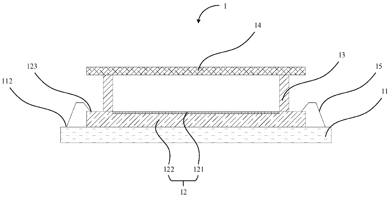
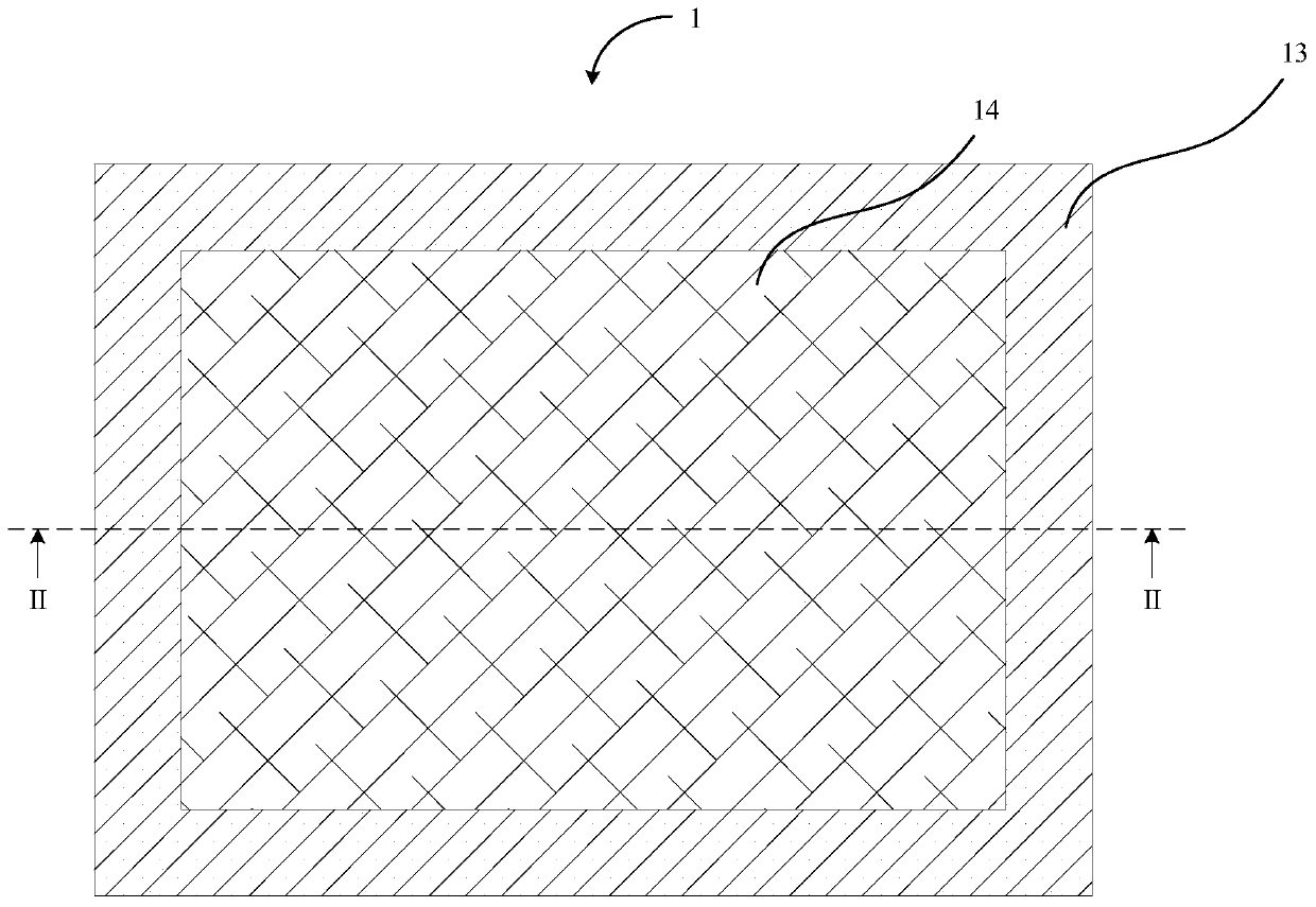
[0037] This application provides an optical chip packaging structure 1, please refer to figure 1 and figure 2 , figure 1 A schematic top view of the optical chip packaging structure provided in the first embodiment of the present application; figure 2 for figure 1 A schematic cross-sectional view along line I-I. The optical chip packaging structure 1 includes: a substrate 11 , a photosensitive element 12 , a support 13 , a first optical device 1...


PUM


Abstract

The invention provides an optical chip packaging structure, a packaging method thereof and a photoelectric device. The optical chip packaging structure comprises a substrate; a photosensitive element,wherein the photosensitive element is borne on the substrate; a support body which abuts against a substrate, or the support body is arranged on the photosensitive element; a first optical device, wherein the first optical device and the supporting body are of an integrated structure, and the first optical device is borne on the side, away from the photosensitive element, of the supporting body;and a lead, wherein the first welding point of the photosensitive element is electrically connected with a circuit in the substrate through the lead. The optical chip packaging structure formed by supporting the optical device through the supporting body is simple and reliable, the technological manufacturing process of the optical chip packaging structure is simple, and the manufacturing cost iseffectively reduced. Due to the fact that the optical chip packaging structure is simple, wiring, calibration and the like of the optical chip packaging structure can be achieved without complex technologies in the subsequent using process of the optical chip packaging structure.

Description

technical field [0001] The present application relates to the technical field of chip packaging, in particular to an optical chip packaging structure, a packaging method thereof, and an optoelectronic device. Background technique [0002] At present, chips have become one of the most important electronic components in circuit design. In the chip manufacturing process, packaging is one of the main processes. However, due to the optical structure involved in the optical chip, the traditional chip packaging process cannot package the optical chip. The existing optical chip packaging process has high production costs, complicated process flow, and difficult calibration in the subsequent use process. Contents of the invention [0003] The present application discloses an optical chip packaging structure, which can reduce manufacturing cost, has a simple process flow, and is less difficult to calibrate. [0004] In a first aspect, the present application provides an optical c...

Claims


Application Information

Patent Timeline
IPC IPC(8): H01L31/0203H01L31/0232H01L31/18
CPCH01L31/0203H01L31/02327H01L31/18Y02P70/50
Inventor 汤为
Owner SHENZHEN ADAPS PHOTONICS TECH CO LTD
Learn More