
Wafer plastic packaging method, wafer level packaging structure and packaging method thereof, and plastic packaging mold

A technology for plastic packaging molds and wafer-level chips, which is applied in the manufacture of electrical components, circuits, semiconductors/solid-state devices, etc., can solve the problem that the utilization rate of chips needs to be further improved, and achieve the improvement of the problem of plastic packaging eccentricity, increase the utilization rate, and cutting The effect of area reduction

Active Publication Date: 2022-03-11
NINGBO SEMICON INT CORP
View PDF4 Cites 0 Cited by
  • Summary
  • Abstract
  • Description
  • Claims
  • Application Information

AI Technical Summary

Problems solved by technology

[0003] However, the chip utilization rate of the current wafer-level packaging method needs to be further improved

Method used


Image

  • Wafer plastic packaging method, wafer level packaging structure and packaging method thereof, and plastic packaging mold
  • Wafer plastic packaging method, wafer level packaging structure and packaging method thereof, and plastic packaging mold
  • Wafer plastic packaging method, wafer level packaging structure and packaging method thereof, and plastic packaging mold

Examples


Embodiment Construction

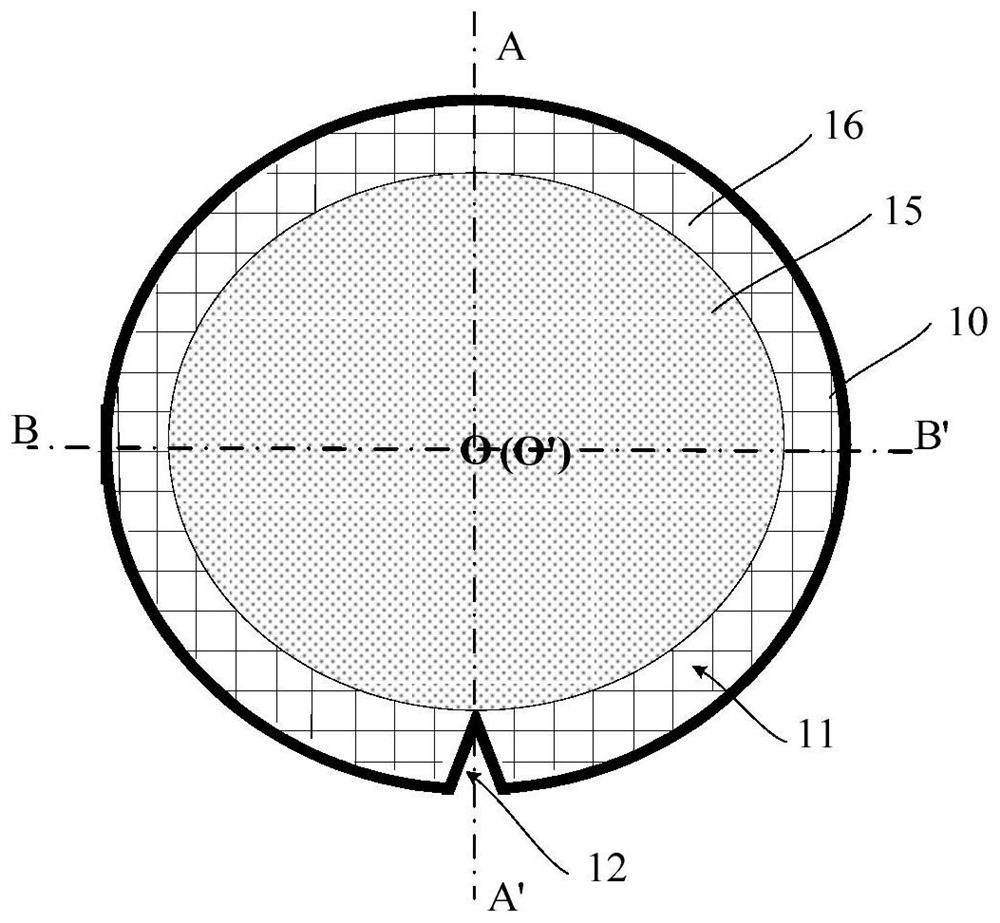
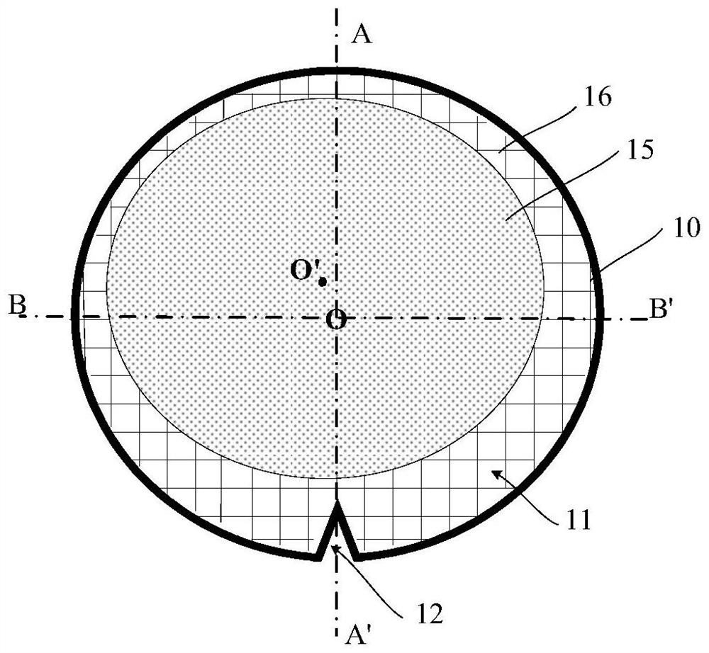
[0057] As we all know, the edge region of the wafer usually has a notch (Notch), which is generally V-shaped, which can be used as a mark for the crystallographic direction of the wafer and plays a role in positioning during the wafer manufacturing process. The inventors found that, in the molding process of wafer level packaging (Wafer Level Package, WLP), when the molding compound (MoldingCompound) on the wafer is heated and pressed until it is close to the size of the wafer, the molding compound will be released from the edge of the wafer. The V-notch overflows. Due to the limitation of the gap on the wafer, in actual molding, the area covered by the molding material on the wafer (that is, the molding area) is often smaller than the area of ​​the wafer to avoid overflow of the molding material.

[0058] Figure 1a It is a schematic diagram of the structure of wafer plastic packaging without eccentricity in the existing process, Figure 1b It is a schematic diagram of the s...


PUM

PropertyMeasurementUnit
thicknessaaaaaaaaaa

Abstract

The invention provides a wafer plastic packaging method, a wafer-level packaging structure and its packaging method, and a plastic packaging mold. The wafer carrying the plastic packaging material is placed on the first template of the plastic packaging mold, and the second template of the plastic packaging mold passes through the wafer. applying pressure to the molding material to form a molding layer on the surface of the wafer facing away from the first template, wherein a protrusion is formed on the surface of the second template of the molding mold facing the wafer, so When the second template applies pressure to the molding compound, the protrusion is located above the notch and is used to prevent the molding compound from overflowing from the notch, so that a larger area of ​​molding can be achieved, and the problem of eccentric molding can be improved, and The area to be cut in the subsequent trimming process is reduced, which is beneficial to improving the utilization rate of effective chips on the wafer.

Description

technical field [0001] The invention relates to the technical field of semiconductor packaging, in particular to a wafer plastic packaging method, a wafer-level packaging structure and packaging method thereof, and a plastic packaging mold. Background technique [0002] With the development trend of very large scale integrated circuits, the feature size of integrated circuits continues to decrease, and people's requirements for packaging technology of integrated circuits continue to increase accordingly. Existing packaging technologies include system-in-package (System inPackage, SIP), system-on-chip (System on chip, SOC) packaging, wafer-level packaging (Wafer Level Package, WLP) and the like. SIP is a combination of multiple active components, passive components, and optical components with different functions into one unit to form a system or subsystem that can provide multiple functions, which allows heterogeneous IC integration and is commonly used A packaging integrat...

Claims


Application Information

Patent Timeline
Patent Type & Authority Patents(China)
IPC IPC(8): H01L21/56
CPCH01L21/56H01L21/565
Inventor 石虎李海江敖萨仁李洪昌孙尧中
Owner NINGBO SEMICON INT CORP
Learn More