A hole pattern electroplating method for fpc
A graphic electroplating and partial plating technology, which is applied in the manufacture of printed circuits, electrical components, printed circuits, etc., to achieve the effects of reducing height, improving the yield rate of circuit production, and improving the effect of poor clamping film
- Summary
- Abstract
- Description
- Claims
- Application Information
AI Technical Summary
Problems solved by technology
Method used
Image
Examples
Embodiment Construction
[0026] In order to further explain the technical solution of the present invention, the present invention will be described in detail below through specific examples.
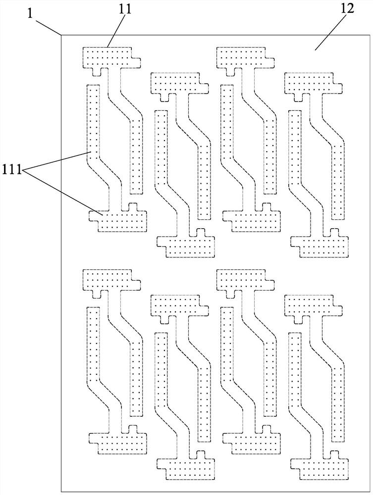
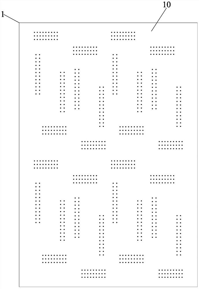
[0027] Such as Figure 4 to Figure 7 Shown, the present invention is a kind of hole pattern electroplating method of FPC, and its technological process comprises the following steps:
[0028] Step A: Laminating the dry film on the substrate, and laminating the dry film on both sides of the top and bottom layers of the substrate 2 to be partially copper-plated;
[0029] Step B: Partial exposure. Expose the top and bottom layers of the substrate 2 obtained in step A, and transfer the exposure of the partial dry film pattern 20 of the unit hole to the top and bottom dry films corresponding to all FPC unit product areas in the substrate 2. The FPC unit product The area 22 of jigsaw waste outside 21 is not exposed;
[0030] Step C: Partial development, developing the substrate 2 obtained in step B to form a local ...
PUM
 Abstract
Description
Claims
Application Information
 - R&D Engineer
- R&D Manager
- IP Professional
- Industry Leading Data Capabilities
- Powerful AI technology
- Patent DNA Extraction
Browse by: Latest US Patents, China's latest patents, Technical Efficacy Thesaurus, Application Domain, Technology Topic, Popular Technical Reports.
© 2024 PatSnap. All rights reserved.Legal|Privacy policy|Modern Slavery Act Transparency Statement|Sitemap|About US| Contact US: help@patsnap.com


