Method for processing precise light sensitive hole through ultrasonic laser processing and laser equipment
An ultraviolet laser and processing method technology, applied in laser welding equipment, metal processing equipment, welding equipment and other directions, can solve the problems of complicated silk screen processing hole process, poor light transmission effect, large aperture of photosensitive hole and so on
- Summary
- Abstract
- Description
- Claims
- Application Information
AI Technical Summary
Problems solved by technology
Method used
Image
Examples
Embodiment 1
[0111] Processed piece: mobile phone glass panel with a thickness of 0.8mm, its surface ink thickness is 0.03mm, the diameter of the processed hole is set to 0.03mm, the number is 700 (circular array), and the distance between adjacent processed holes is 0.1mm.
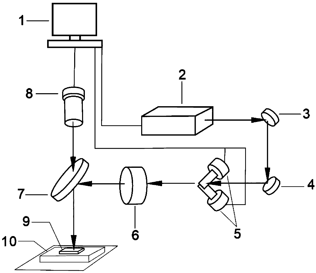
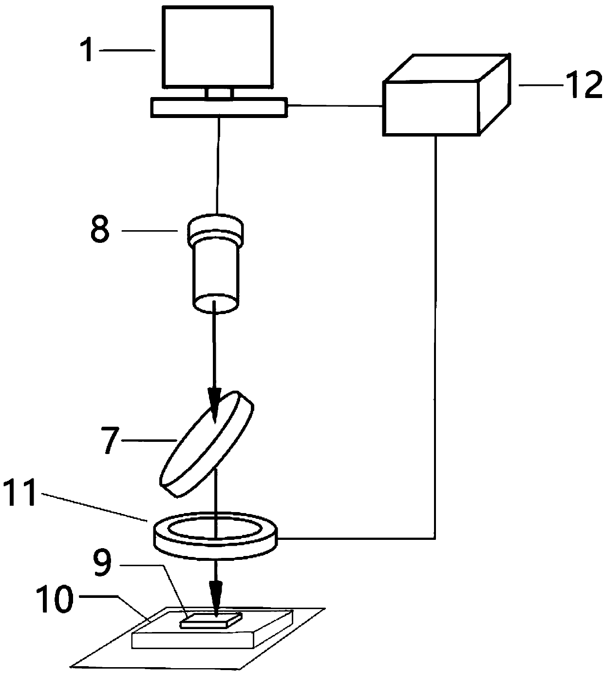
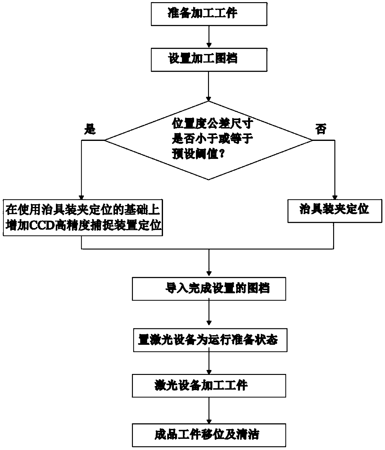
[0112] The operation steps for ultra-violet laser efficient processing of precision photosensitive holes are as follows:
[0113] (1) Workpiece clamping and positioning
[0114] Check whether the tolerance size of the jig position meets the production tolerance, decide whether to add a CCD capture and positioning device, and clamp the workpiece flat on the jig.
[0115] (2) Processing graphics processing
[0116] According to the processing requirements, the graphic files of the processed holes should be processed. The graphic design of the micro-holes should have a diameter of 20 μm, a hole spacing of 90 μm, and a circular array of micro-holes, and generate corresponding files.
[0117] (3) Import the processing m...
Embodiment 2
[0123] Processed piece: mobile phone glass panel with a thickness of 0.6mm, the surface ink thickness is 0.02mm, the diameter of the processed hole is set to 0.02mm, the number is 900 (circular array), and the distance between adjacent processed holes is 0.08mm.
[0124] The operation steps for ultra-violet laser efficient processing of precision photosensitive holes are as follows:
[0125] (1) Workpiece clamping and positioning
[0126] Check whether the tolerance size of the jig position meets the production tolerance, decide whether to add a CCD capture and positioning device, and clamp the workpiece flat on the jig.
[0127] (2) Processing graphics processing
[0128] According to the processing requirements, process the graphic files of the processed holes. The graphic design aperture of the micro-holes should be 15 μm, the hole spacing should be 50 μm, and the micro-holes are in a circular array, and the corresponding files are generated.
[0129] (3) Import the proc...
Embodiment 3
[0135] Processed piece: mobile phone glass panel with a thickness of 0.5mm, the surface ink thickness is 0.02mm, the diameter of the processed hole is set to 0.02mm, the number is 1000 (rectangular array), and the distance between adjacent processed holes is 0.08mm.
[0136] The operation steps for ultra-violet laser efficient processing of precision photosensitive holes are as follows:
[0137] (1) Workpiece clamping and positioning
[0138] Check whether the tolerance size of the jig position meets the production tolerance, decide whether to add a CCD capture and positioning device, and clamp the workpiece flat on the jig.
[0139] (2) Processing graphics processing
[0140] According to the processing requirements, process the graphic files of the processed holes. The graphic design aperture of the micro-holes should be 15 μm, the hole spacing should be 50 μm, and the micro-holes are in a circular array, and the corresponding files are generated.
[0141] (3) Import the ...
PUM
| Property | Measurement | Unit |
|---|---|---|
| wavelength | aaaaa | aaaaa |
| thickness | aaaaa | aaaaa |
| thickness | aaaaa | aaaaa |
Abstract
Description
Claims
Application Information
 - R&D
- Intellectual Property
- Life Sciences
- Materials
- Tech Scout
- Unparalleled Data Quality
- Higher Quality Content
- 60% Fewer Hallucinations
Browse by: Latest US Patents, China's latest patents, Technical Efficacy Thesaurus, Application Domain, Technology Topic, Popular Technical Reports.
© 2025 PatSnap. All rights reserved.Legal|Privacy policy|Modern Slavery Act Transparency Statement|Sitemap|About US| Contact US: help@patsnap.com


