Method, device and electronic equipment for calibrating chip wireless parameters

A wireless parameter and calibration method technology, which is applied in the field of wireless transmission, can solve problems such as the accuracy being affected by the environment, the deviation of individual chip results, and the cumbersome process

Active Publication Date: 2020-12-29
ASR MICROELECTRONICS (SHENZHEN) CO LTD
View PDF3 Cites 0 Cited by
  • Summary
  • Abstract
  • Description
  • Claims
  • Application Information

AI Technical Summary

Problems solved by technology

The initial wireless power of the same batch of chips tends to be consistent as a whole, and the results of individual chips are biased due to the influence of the environment
According to the actual practice of the factory in the past, it will try to reduce the change of the environment to reduce the deviation, but it will cause certain restrictions on production.
[0003] It can be seen that the existing chip wireless parameter calibration scheme has technical problems such as cumbersome process or the accuracy is affected by the environment

Method used


Image

  • Method, device and electronic equipment for calibrating chip wireless parameters
  • Method, device and electronic equipment for calibrating chip wireless parameters
  • Method, device and electronic equipment for calibrating chip wireless parameters

Examples


Embodiment Construction

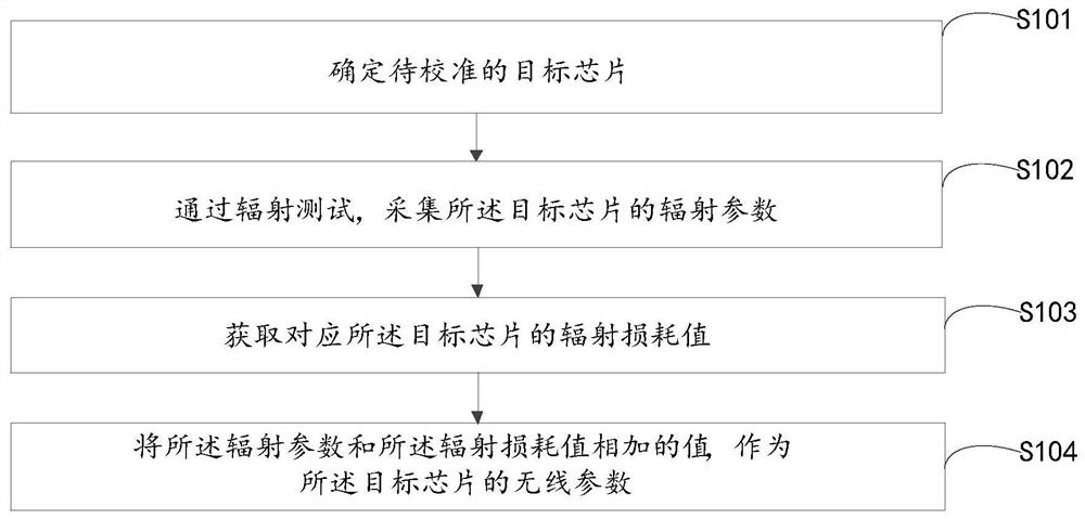
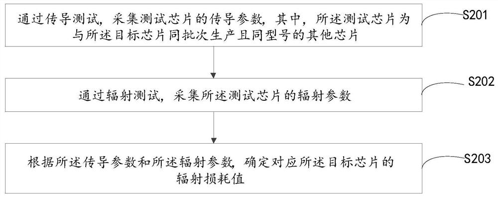
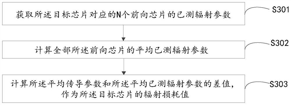
[0055] Embodiments of the present disclosure will be described in detail below in conjunction with the accompanying drawings.

[0056] Embodiments of the present disclosure are described below through specific examples, and those skilled in the art can easily understand other advantages and effects of the present disclosure from the contents disclosed in this specification. Apparently, the described embodiments are only some of the embodiments of the present disclosure, not all of them. The present disclosure can also be implemented or applied through different specific implementation modes, and various modifications or changes can be made to the details in this specification based on different viewpoints and applications without departing from the spirit of the present disclosure. It should be noted that, in the case of no conflict, the following embodiments and features in the embodiments can be combined with each other. Based on the embodiments in the present disclosure, a...


PUM


Abstract

The embodiment of the invention provides a chip wireless parameter calibration method and device, and electronic equipment, which belongs to the technical field of wireless transmission. The method comprises the steps of determining a to-be-calibrated target chip; acquiring a radiation loss value corresponding to the target chip; acquiring radiation parameters of the target chip through a radiation test; and taking a value obtained by adding the radiation parameter and the radiation loss value as a wireless parameter of the target chip. Through the scheme of the invention, the calibration process of the wireless parameters of the chip is simplified; the loss caused by environmental factors in the radiation test process is compensated, and the accuracy of wireless parameter calibration is improved; emission parameter calibration deviation caused by environmental factors during radiation calibration in production calibration of the wireless signal emission chip is weakened; and the method is convenient for batch processing and production, so that wireless emission calibration of factory chips is more accurate.

Description

technical field [0001] The present disclosure relates to the technical field of wireless transmission, in particular to a method, device and electronic equipment for calibrating wireless parameters of a chip. Background technique [0002] Existing calibration methods for chip wireless parameters mainly include conduction testing and radiation testing. Among them, the conduction test is through a wired connection, and the line loss is fixed and it is not easy to have deviations, but the test process is relatively cumbersome. The radiation test refers to the wireless measurement of the parameters of the radio frequency port of the chip, and the line loss is easily affected by the environment. The initial wireless power of the same batch of chips tends to be consistent as a whole, and the results of individual chips are biased due to the influence of the environment. According to the actual practice of the factory in the past, the change of the environment will be minimized t...

Claims


Application Information

Patent Timeline
Patent Type & Authority Patents(China)
IPC IPC(8): H04B17/11H04B17/21
CPCH04B17/11H04B17/21
Inventor 祖东辉刘森叶红亮
Owner ASR MICROELECTRONICS (SHENZHEN) CO LTD
Why Eureka
Try Eureka