High-speed optical delay line chip and device

An optical delay line and chip technology, applied in the field of optical delay lines, can solve the problems of slow scanning speed and large size of optical delay line devices, achieve fast switching speed, realize large-scale integrated design, and improve the effect of coupling efficiency

Pending Publication Date: 2020-05-15
杭州洛微科技有限公司
View PDF2 Cites 0 Cited by
  • Summary
  • Abstract
  • Description
  • Claims
  • Application Information

AI Technical Summary

Problems solved by technology

[0009] The present invention mainly solves the problems of large volume and slow scanning speed of optical delay line devices in the prior art, and provides a high-speed optical delay line chip and device. The present invention has the advantages of miniaturization, light weight and fast scanning speed

Method used


Image

  • High-speed optical delay line chip and device
  • High-speed optical delay line chip and device
  • High-speed optical delay line chip and device

Examples


Embodiment 1

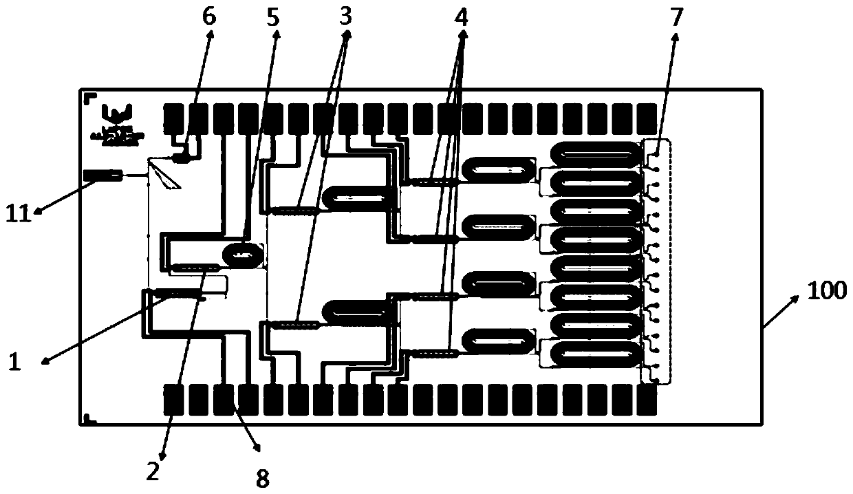
[0036] figure 1 is a schematic structural diagram of the high-speed optical delay line chip 100 .

[0037] like figure 1 As shown, in order to solve the above problems, an embodiment of the present invention provides a high-speed optical delay line chip 100, including:

[0038] Channel selection module, detector module 6, ring waveguide module 5 and closed-loop reflective waveguide module 7; the channel selection module includes N-level thermo-optic switches, wherein: the first-level to N-1th-level thermo-optic switches are MZ-MMI thermo-optic switches switch, the Nth-stage thermo-optic switch is a 1×2MMI thermo-optic switch; the input end 11 of the first-stage thermo-optic switch is an external fiber laser light source coupled to the planar waveguide of the chip, and the first output end of the first-stage thermo-optic switch is connected to The detector module 6, the second output end of the first-stage thermo-optic switch is connected to the input end of the second-stage ...

Embodiment 2

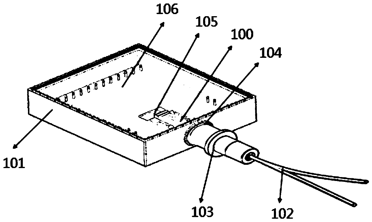
[0050] image 3 is a schematic diagram of the structure of a high-speed optical delay line device.

[0051] like image 3 As shown, the present invention also discloses a high-speed delay line device, including:

[0052] Any one of the above high-speed optical delay line chip 100, housing 101, optical fiber 102, optical fiber 102 socket 103, lens 104, substrate 105 and power supply module 106, wherein: the optical fiber 102 socket 103 is arranged outside the housing 101, the optical fiber 102 and the optical fiber 102 socket 103 connection, used to transmit the laser fiber light source to the lens 104, the lens 104 is arranged between the optical fiber 102 socket 103 and the housing 101, for coupling the laser fiber light source to the high-speed optical delay line chip 100 planar waveguide place, the substrate 105 is arranged inside the casing 101, and the high-speed optical delay line chip 100 is arranged on the substrate 105, and is connected with the power supply module ...


PUM

PropertyMeasurementUnit
refractive indexaaaaaaaaaa

Abstract

The invention discloses a high-speed optical delay line chip and device. The high-speed optical delay line chip comprises a channel selection module, a detector module, an annular waveguide module anda closed-loop reflection waveguide module. The channel selection module comprises N stages of thermo-optical switches, wherein the first stage to the (N-1) th stage thermo-optical switches are MZ-MMIthermo-optical switches, and the Nth stage thermo-optical switch is a 1 * 2 MMI thermo-optical switch; the high-speed optical delay line device comprises the high-speed optical delay line chip, a shell, an optical fiber, an optical fiber socket, a lens, a substrate and a power supply module, wherein the optical fiber socket is arranged on the outer side of the shell, the optical fiber is connected with the optical fiber socket, the lens is arranged between the optical fiber socket and the shell, the substrate is arranged in the shell, and the high-speed optical delay line chip is arranged onthe substrate and connected with the power supply module arranged in the shell. The advantages of miniaturization, light weight and high scanning speed can be realized.

Description

technical field [0001] The invention relates to the field of optical delay lines, in particular to a high-speed optical delay line chip and device. Background technique [0002] An optical delay line is an optical device that changes the optical path or phase. It is necessary to use an optical delay line to change the optical path or phase in equipment or measuring instruments that use the principle of optical interference, so that the two-arm optical path that interferes meets the The principle of light interference. Most of the optical interferometry techniques that have emerged in recent years use the principle of broadband interferometry, which can be roughly divided into two categories, one is partially coherent interferometry (PCI), and the other is weakly coherent reflectometry (LCR). [0003] For example, "Interference Arrangement of Diffractive Optical Elements for Measuring Intraocular Distance", the publication number is US5673096A, and the publication date is Se...

Claims


Application Information

Patent Timeline
Patent Type & Authority Applications(China)
IPC IPC(8): G02B6/28G02B6/293G02B6/32
CPCG02B6/2861G02B6/29344G02B6/32
Inventor 孙笑晨冯宁宁刘飞
Owner 杭州洛微科技有限公司
Why Eureka
Try Eureka