Signal jitter estimation method for the output of lpddr4 IO interface

A technology of LPDDR4IO and output terminal, applied in the direction of calculation, design optimization/simulation, CAD numerical modeling, etc., to achieve the effect of high accuracy and rich frequency domain details

Active Publication Date: 2021-08-20
XIDIAN UNIV
View PDF10 Cites 0 Cited by
  • Summary
  • Abstract
  • Description
  • Claims
  • Application Information

AI Technical Summary

Problems solved by technology

[0009] The purpose of the present invention is to address the above-mentioned deficiencies in the prior art, and propose a signal jitter estimation method for the output of the LPDDR4 IO interface for the signal jitter caused by the noise of the power supply rail, and solve how to use the numerical calculation method to quickly and accurately LPDDR4 The problem of jitter estimation caused by power supply noise in the IO link can be applied in actual engineering

Method used


Image

  • Signal jitter estimation method for the output of lpddr4 IO interface
  • Signal jitter estimation method for the output of lpddr4 IO interface
  • Signal jitter estimation method for the output of lpddr4 IO interface

Examples


Embodiment Construction

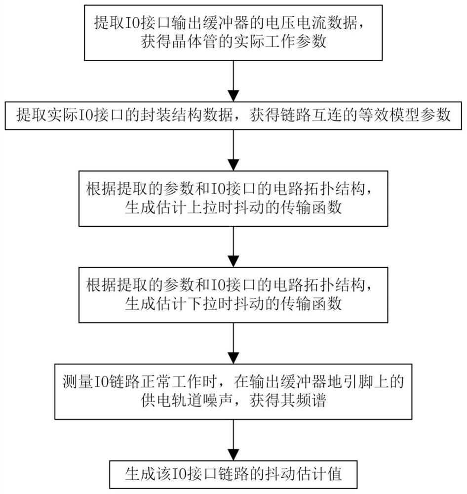
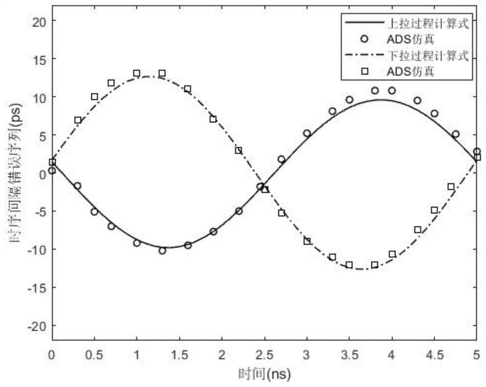
[0055] The present invention will be further described below in conjunction with the accompanying drawings.

[0056] Refer to attached figure 1 , to further describe the specific steps of the present invention.

[0057] Step 1, obtaining the actual working parameters of the MOS tube.

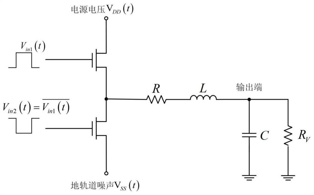
[0058] The first step is to extract the working data of the output device used in the actual LPDDR4 IO interface link, and draw the current and voltage working curves of the pull-up NMOS and the pull-down NMOS.

[0059] The second step is to obtain the DC operating point voltage V of the pull-up NMOS transistor according to the current-voltage curve of the pull-up NMOS. 0 , DC transconductance g dc and small signal AC transconductance g m .

[0060] Specific steps are as follows:

[0061] In the first step, the center point of the maximum and minimum values ​​of the gate-source voltage when the pull-up NMOS is working is taken as the DC operating point voltage V 0 .

[0062] Step 2, find...


PUM


Abstract

A method for estimating signal jitter at the output end of an LPDDR4 IO interface, which mainly solves the problem in the prior art that there is no simple numerical calculation method for estimating the signal timing jitter caused by the noise of its power supply rail for an LPDDR4 IO interface with a dual NMOS structure . The steps that the present invention realizes are as follows, (1) obtain the actual working parameter of MOS tube; (2) obtain the equivalent model parameter of link interconnection; (3) generate the transfer function that the output end jitters when estimating pull-up; (4) Generate a transfer function for estimating the output jitter during pull-down; (5) Obtain the ground track noise spectrum when the interface link is working; (6) Generate an estimated jitter value for the LPDDR4 IO interface link. The invention adopts a numerical calculation method, which saves time compared with a software simulation method, and the generated transfer function has richer frequency domain details.

Description

technical field [0001] The invention belongs to the technical field of electronic circuits, and further relates to an IO interface (Input) for the fourth-generation low-power double-rate synchronous dynamic random access memory LPDDR4 (Low-power double data ratefourth generation) in high-speed circuit signal analysis technology / Output Interface) output signal jitter estimation method. The invention can be used for estimating timing jitter in the process of high-speed circuit data transmission and participates in the design of power supply distribution network for suppressing power supply track noise. Background technique [0002] The timing jitter of a digital signal refers to the deviation between the actual signal edge time and the ideal edge time position. Excessive deviation will distort the signal level sampled by the receiver and generate bit errors. The noise sources that cause deterministic timing jitter mainly include crosstalk, power supply rail noise, rising edg...

Claims


Application Information

Patent Timeline
Patent Type & Authority Patents(China)
IPC IPC(8): G06F30/20G06F111/10G06F17/15
CPCG06F17/15G06F17/156
Inventor 刘洋夏铭泽曾操孙肖杨朱磊磊
Owner XIDIAN UNIV
Why Eureka
Try Eureka