
Charging and discharging MOS protection circuit

A protection circuit, charge and discharge technology, applied in safety/protection circuits, emergency protection circuit devices, battery circuit devices, etc., can solve the problem of damage to mos tubes, etc.

Pending Publication Date: 2020-04-17
苏州妙益科技股份有限公司
View PDF0 Cites 0 Cited by
  • Summary
  • Abstract
  • Description
  • Claims
  • Application Information

AI Technical Summary

Problems solved by technology

[0003] In the charging and discharging project of the battery, if there is no protection, when the charging MOS or discharging MOS is cut off at high current, a back pressure will be formed according to the circuit theory. When the back pressure exceeds the withstand voltage of the MOS tube, the MOS tube will be damaged.

Method used


Image

  • Charging and discharging MOS protection circuit

Examples


Embodiment Construction

[0013] The present invention will be further described below in conjunction with accompanying drawing.

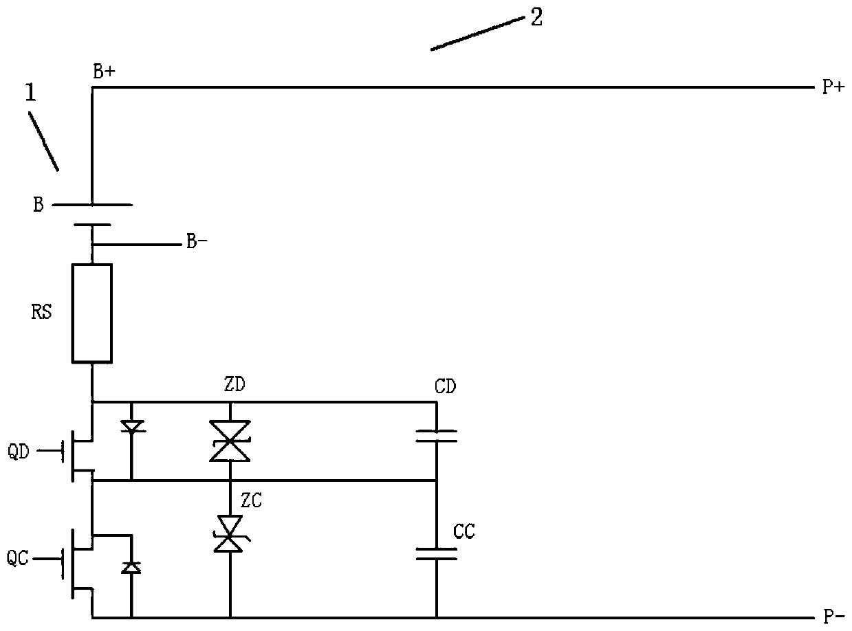
[0014] according to figure 1 A charging and discharging MOS protection circuit of the present invention is shown, including a battery 1 and a protection circuit 2. The protection circuit 2 includes a current sampling resistor RS, a discharge control mosQD, a charge control mosQC, and a discharge mos protection regulator ZD, Discharging MOS protection capacitor CD, charging MOS protection regulator ZC, and charging MOS protection capacitor CC, wherein the current sampling resistor RS is used for measuring current by the CPU, and the discharge MOS protection regulator ZD and charging MOS protection regulator ZC Provide voltage limiting protection. When the back pressure caused by cutting off the MOS exceeds the limit voltage of the discharge MOS protection regulator ZD and the charge MOS protection regulator ZC, the discharge MOS protection regulator ZD and the charge MOS pro...


PUM


Abstract

The invention discloses a charging and discharging MOS protection circuit. The charging and discharging MOS protection circuit comprises a battery and a protection circuit. The protection circuit comprises a current sampling resistor RS, a discharge control mosQD and a charge control mosQC. The protection circuit also comprises a discharge mos protection voltage-regulator tube ZD, a discharge mosprotection capacitor CD, a charge mos protection voltage-regulator tube ZC, and a charge mos protection capacitor CC, wherein the current sampling resistor RS is used for measuring current by a CPU; and the discharge mos protection voltage-regulator tube ZD and the charge mos protection voltage-regulator tube ZC provide voltage-limiting protection. According to the invention, the discharge mos protection capacitor CD and the charge mos protection capacitor CC have peak absorption capability; the capacitors are matched with the discharge mos protection voltage-regulator tube ZD and the charge mos protection voltage-regulator tube ZC to protect a mos, the faster the cut-off is, the higher the back voltage is, and after the mos is cut off, the change rate of the current is reduced by chargingand discharging the capacitors, so that the back voltage is reduced.

Description

technical field [0001] The invention relates to the technical field of battery charge and discharge, in particular to a charge and discharge MOS protection circuit. Background technique [0002] MOS tube is the abbreviation of MOSFET. MOSFET metal-oxide semiconductor field effect transistor, referred to as metal oxide semiconductor field effect transistor, is generally a metal (metal) - oxide (oxide) - semiconductor (semiconductor) field effect transistor, or called a metal - insulator (insulator) - semiconductor . The source (source) and drain (depletion layer) of the MOS tube can be reversed, and they are all N-type regions formed in the P-type backgate. In most cases, the two regions are the same, even if the two ends are reversed, it will not affect the performance of the device. Such devices are considered symmetrical. Field effect transistors are divided into PMOS transistors and NMOS transistors, which belong to insulated gate field effect transistors. [0003] I...

Claims


Application Information

Patent Timeline
Patent Type & Authority Applications(China)
IPC IPC(8): H02J7/00H02H3/08H02H7/20
CPCH02H3/08H02H7/205H02J7/0029
Inventor 禹成海
Owner 苏州妙益科技股份有限公司
Learn More