Liquid crystal writing film local erasing voltage loading control method

A technology of erasing voltage and control method, applied in the direction of electrical digital data processing, instrument, data processing input/output process, etc., can solve the problem of excessive capacitance of liquid crystal writing film, uneven thickness of glue coating, and partial erasure Effect and other issues, to achieve the effect of improving the yield, reducing the quality and the requirements of processing accuracy

Inactive Publication Date: 2020-03-27
SHANDONG LANBEISITE EDUCATIONAL EQUIP GRP +1
View PDF0 Cites 4 Cited by
  • Summary
  • Abstract
  • Description
  • Claims
  • Application Information

AI Technical Summary

Problems solved by technology

This puts forward high requirements on the quality and processing accuracy of the liquid crystal writing film. If the liquid crystal thickness of the produced liquid crystal writing film is too high or the thickness of the coating glue is too high or uneven, it will cause the liquid crystal writing film to die due to excessive capacitance. Affect the partial erasing effect, which reduces the yield of liquid crystal writing film to a certain extent

Method used


Image

  • Liquid crystal writing film local erasing voltage loading control method
  • Liquid crystal writing film local erasing voltage loading control method
  • Liquid crystal writing film local erasing voltage loading control method

Examples


Embodiment 1

[0055] Based on the above description of the problems in the prior art, the embodiment of the present invention discloses a method for controlling voltage loading for local erasing of a liquid crystal writing film. This embodiment introduces a method for controlling voltage loading during voltage boosting.

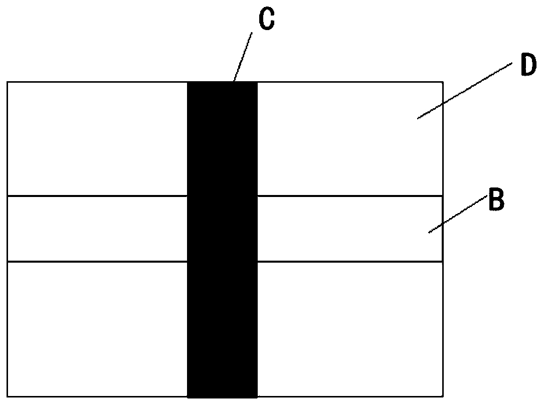
[0056] Wherein, the liquid crystal writing film is located between two conductive layers, and the two conductive layers are respectively divided into two or more than two conductive regions. In this embodiment, the first conductive layer is divided into two or more lateral conductive regions that are insulated from each other, and the second conductive layer is divided into two or more vertical conductive regions that are insulated from each other; The conductive regions on the second conductive layer and the conductive regions on the second conductive layer are vertically interlaced with each other in space. By dividing the conductive layer, the writing film is divided in...

Embodiment 2

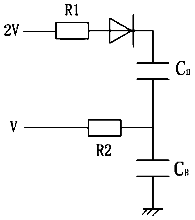
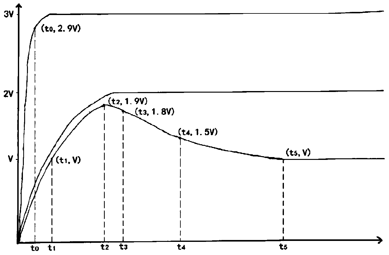
[0087] In some other embodiments, a method for controlling the partial erasing voltage step-down process is disclosed, such as Figure 7 As shown, it specifically includes the following process:

[0088] (1) The voltage of the conductive area covering the partial erasing area on the first conductive layer is reduced from 3Va to Va, so that the absolute value of the voltage difference between each set conductive area on the two conductive layers is Va;

[0089] (2) The voltage of each set conductive area on the second conductive layer is reduced from 2Va to zero, and the absolute value of the voltage difference between each set conductive area on the two conductive layers is still Va;

[0090] (3) The voltage of each set conductive area on the first conductive layer is reduced from Va to zero, and the voltage difference between all set conductive areas on the two conductive layers is zero.

[0091] It can be seen that during the step-by-step step-down process, the voltage diff...

Embodiment 3

[0095] On the basis of Embodiment 1, the embodiment of the present invention discloses a liquid crystal writing film using a local erasing voltage loading control method, and specific application products of the writing film, such as:

[0096]The liquid crystal writing film adopting the local erasing voltage generation and control method of the present invention is applied to a writing board, a drawing board or a blackboard to realize the local erasing function.


PUM


Abstract

The invention discloses a liquid crystal writing film local erasing voltage loading control method. The method comprises: increasing the voltage of a set conductive area on a first conductive layer toa first auxiliary voltage A; increasing the voltage of a set conductive region on the second conductive layer to a second auxiliary voltage B; adjusting the voltage of the conductive region coveringthe local erasure region on the first conductive layer to be C, and adjusting the voltage of the conductive region covering the local erasure region on the second conductive layer to be D; enabling the voltage difference between the conductive regions covering the local erasure regions on the two conductive layers to form an erasure electric field, wherein the electric field formed by the voltagedifference between the two conductive layers outside the local erasure regions cannot cause the liquid crystal indentation to visually become shallow or disappear. Through a step-by-step voltage boosting and step-by-step voltage reducing mode, the influence of the capacitance effect of the liquid crystal writing film is reduced, meanwhile, the requirements for the quality and the machining precision of the liquid crystal writing film are reduced, and the yield of the liquid crystal writing film is increased.

Description

technical field [0001] The invention relates to the technical field of liquid crystal film structure, in particular to a method for controlling local erasing voltage loading of a liquid crystal writing film. Background technique [0002] The working principle of the liquid crystal writing film currently on the market is to use the bistable characteristics of liquid crystals to display and / or erase the written content on the liquid crystal writing board. For example, using cholesteric liquid crystal as a writing film, the writing pressure track of the writing pen is recorded by the pressure acting on the liquid crystal writing board, and then the corresponding writing content is displayed; the structure of the cholesteric liquid crystal is changed by applying an electric field, so that the liquid crystal The writing pressure track on the tablet disappears to enable erasing. [0003] The liquid crystal writing film partial erasing voltage control method disclosed in the prior...

Claims


Application Information

Patent Timeline
IPC IPC(8): G06F3/041
CPCG06F3/0412G06F3/0416
Inventor 李清波史新立杨猛训伊西锋张宗梁
Owner SHANDONG LANBEISITE EDUCATIONAL EQUIP GRP
Why Eureka
Try Eureka