Preparation method for LED display device and LED display device

A technology for display devices and LED chips, which is applied to semiconductor devices, static indicators, and electric solid-state devices, etc., can solve the problems of inability to achieve high pixel density LED chip colorization.

Inactive Publication Date: 2020-03-10
CHENGDU VISTAR OPTEOLECTRONICS CO LTD
View PDF10 Cites 0 Cited by
  • Summary
  • Abstract
  • Description
  • Claims
  • Application Information

AI Technical Summary

Problems solved by technology

[0004] In the prior art, inkjet printing is generally used to directly coat the quantum dots on the LED chip to stimulate RGB three-color light, and then realize the colorization of the LED chip through color matching, but due to the printing accuracy Restrictions, unable to achieve colorization of high pixel density LED chips

Method used


Image

  • Preparation method for LED display device and LED display device
  • Preparation method for LED display device and LED display device
  • Preparation method for LED display device and LED display device

Examples


Embodiment Construction

[0026] Certain words are used to refer to specific components in the description and claims, and those skilled in the art should understand that manufacturers may use different terms to refer to the same component. The specification and claims do not use the difference in name as a way to distinguish components, but use the difference in function of components as a basis for distinction. The present invention will be described in detail below in conjunction with the accompanying drawings and embodiments.

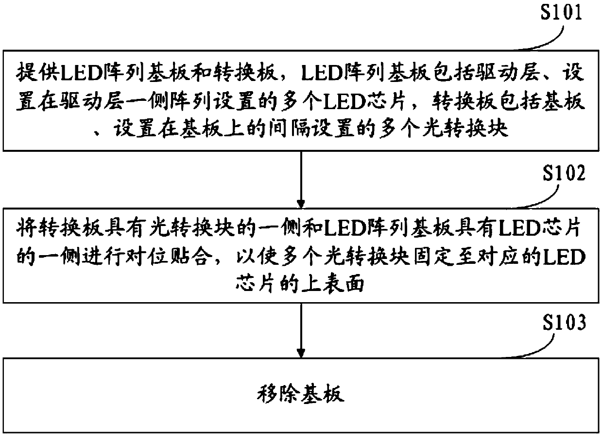
[0027] figure 1 It is a schematic flow chart of the method for manufacturing an LED display device according to the first embodiment of the present invention. It should be noted that if there are substantially the same results, the method of the present invention does not figure 1 The flow sequence shown is limited. Such as figure 1 As shown, the method includes the following steps:

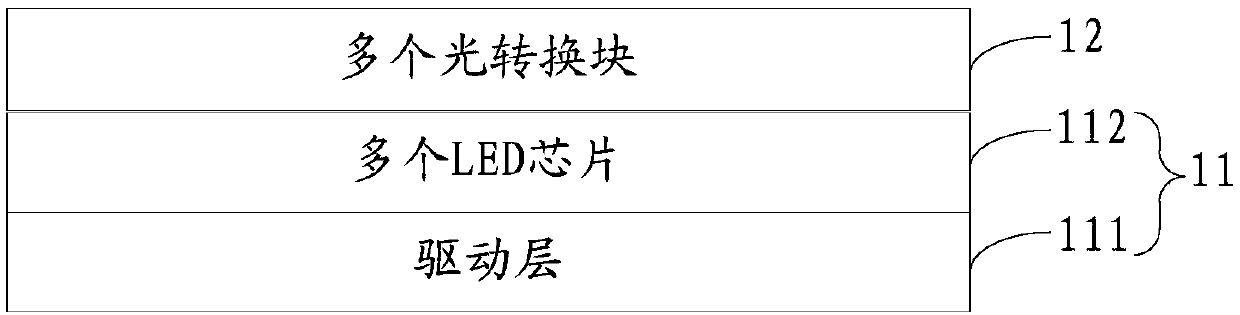
[0028] Step S101: Provide an LED array substrate and a conversion board, the LED array...


PUM


Abstract

The invention discloses a preparation method for an LED display device and the LED display device. The method comprises the steps: an LED array substrate and a conversion plate are provided, wherein the LED array substrate comprises a driving layer and a plurality of LED chips arranged on one side of the driving layer in an array mode, and the conversion plate comprises a substrate and a pluralityof light conversion blocks arranged on the substrate at intervals; the side, provided with the light conversion blocks, of the conversion plate and the side, provided with the LED chips, of the LED array substrate are aligned and attached, so that the multiple light conversion blocks are fixed to the upper surfaces of the corresponding LED chips; and the substrate is removed. In the way, colorization of the high-pixel-density LED chip can be achieved in a relatively simple mode.

Description

technical field [0001] The invention relates to the field of LED display devices, in particular to a method for preparing an LED display device and the LED display device. Background technique [0002] The LED display device includes a plurality of LED chips arranged in an array. The LED chip has the characteristics of self-luminous display, and its technical advantages include all solid state, long life, high brightness, low power consumption, small size, ultra-high Extreme environments such as heat or radiation. At present, the display mode of LED chips is usually monochrome display, and the colorization of LED chips is the key technology for further expanding its application. [0003] As an emerging semiconductor nanocrystalline material, quantum dots have the advantages of high quantum efficiency, precise and adjustable spectrum, and wide color gamut. When applied to displays, they can significantly increase the display color gamut and reduce display power consumption a...

Claims


Application Information

Patent Timeline
Patent Type & Authority Applications(China)
IPC IPC(8): H01L27/15
CPCH01L27/156H01L27/15H01L25/0753H01L2933/0041H01L33/50G09G3/32H01L33/0095H01L33/06H01L33/504H01L2933/0033
Inventor 韦冬杨小龙王建太陈华山
Owner CHENGDU VISTAR OPTEOLECTRONICS CO LTD
Why Eureka
Try Eureka