
Method and device for confirming physical position of failure address in chip storage area

A technology of physical location and storage area, which is applied in the field of confirming the physical location of failure addresses in the chip storage area, can solve the problems of limited accuracy of physical location, failure, bad analysis, etc., and achieve the effect of efficient and accurate physical location marking

Active Publication Date: 2020-01-17
YANGTZE MEMORY TECH CO LTD
View PDF9 Cites 2 Cited by
  • Summary
  • Abstract
  • Description
  • Claims
  • Application Information

AI Technical Summary

Problems solved by technology

[0005] However, the accuracy of the physical location of the failed storage unit found by the existing method is limited, which may easily cause bad analysis failure

Method used


Image

  • Method and device for confirming physical position of failure address in chip storage area
  • Method and device for confirming physical position of failure address in chip storage area
  • Method and device for confirming physical position of failure address in chip storage area

Examples


Embodiment Construction

[0044] As mentioned in the background art, the accuracy of the physical location of the failed storage unit found by the existing method is limited, which easily leads to failure of bad analysis.

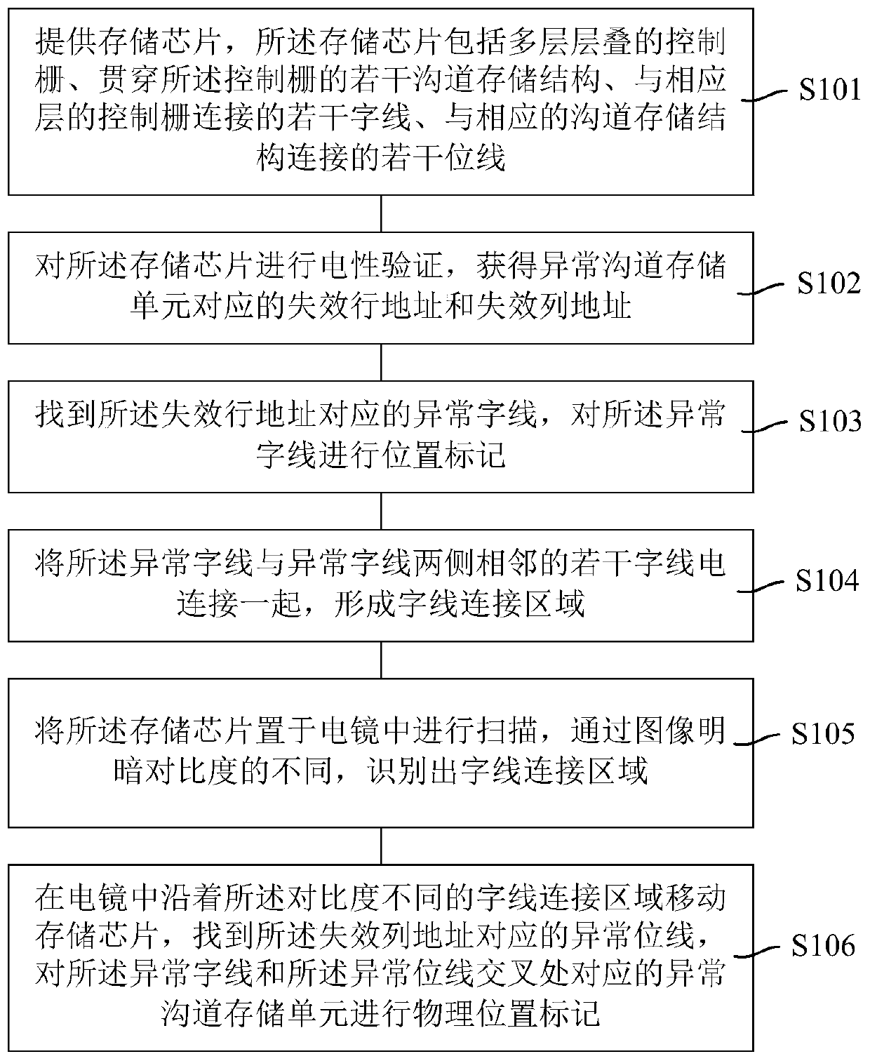
[0045] The study found that the failed row address is generally distinguished at the edge of the storage area, and then moved in parallel to the corresponding failed column address in the electron microscope equipment, and finally the physical address of the failed memory unit is found and marked for slice analysis. However, when the target area is far from the edge of the storage area, the stage of the electron microscope equipment needs to be moved for a long distance, and the long-distance movement of the electron microscope equipment stage is prone to deviation, resulting in incorrect addresses and analysis failures.

[0046] To this end, the present invention provides a method and device for confirming the physical location of a failure address in a chip storage area of ​​the pr...


PUM


Abstract

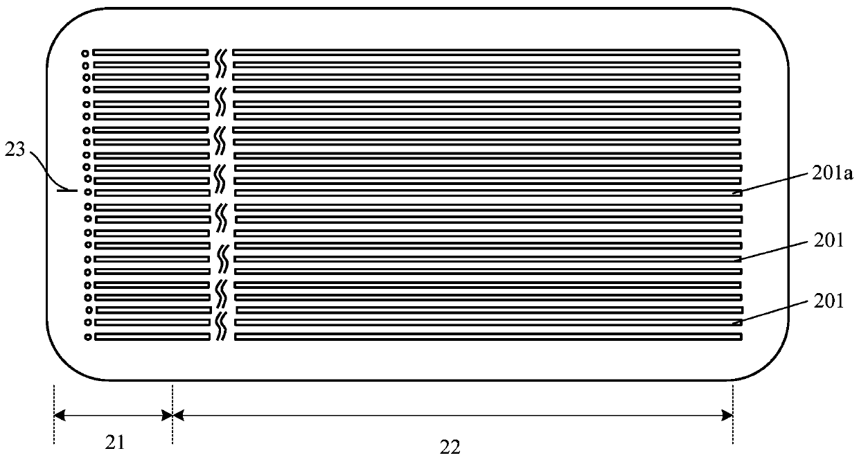
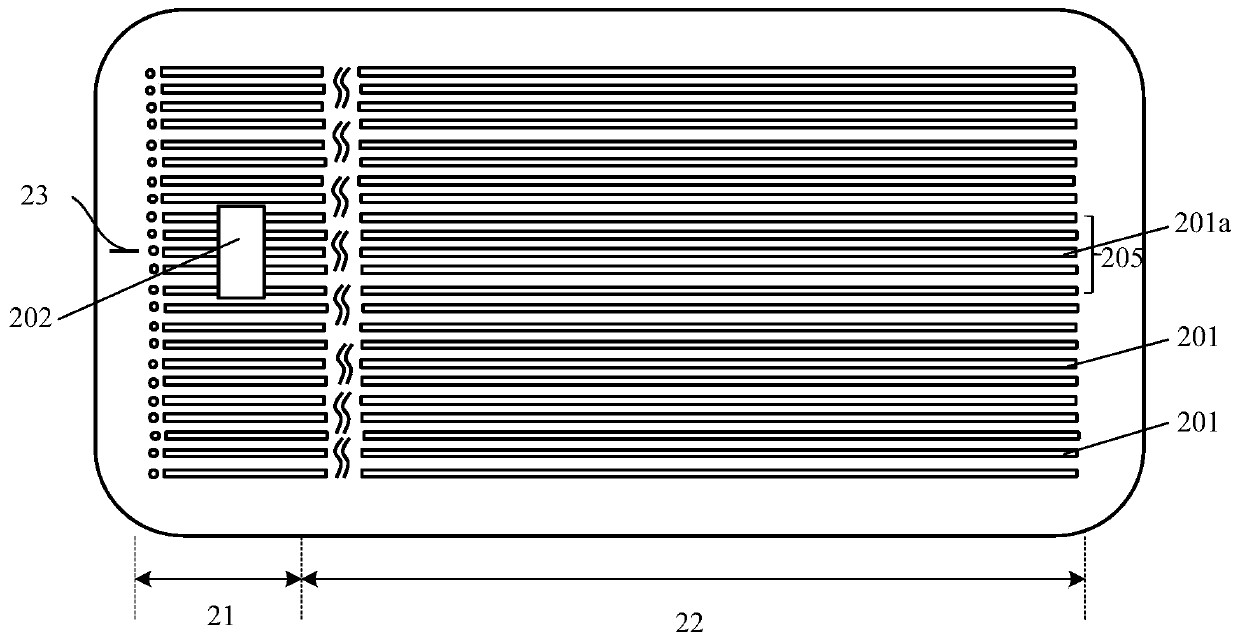
The invention discloses a method and a device for confirming the physical position of a failure address in a chip storage area, and the method comprises the steps: carrying out the electrical verification of a storage chip, obtaining a failure row address and a failure column address corresponding to an abnormal channel storage unit, finding an abnormal word line corresponding to the failure row address, and carrying out the position marking of the abnormal word line; electrically connecting the abnormal word line with a plurality of adjacent word lines on two sides of the abnormal word line to form a word line connection area; placing the memory chip in an electron microscope for scanning, and identifying a word line connection area according to different image light and shade contrast ratios; and moving a memory chip along the word line connection areas with different contrasts in an electron microscope, finding an abnormal bit line corresponding to the failure column address, and performing physical position marking on an abnormal channel memory unit corresponding to the intersection of the abnormal word line and the abnormal bit line. According to the method, the accuracy of physical position marking is improved.

Description

technical field [0001] The invention relates to the field of semiconductor manufacturing, in particular to a method and device for confirming the physical location of a failure address in a chip storage area. Background technique [0002] NAND flash memory is a better storage device than hard disk drives, and it has been widely used in electronic products as people pursue non-volatile storage products with low power consumption, light weight and high performance. At present, the NAND flash memory with a planar structure is close to the limit of practical expansion. In order to further increase the storage capacity and reduce the storage cost per bit, a 3D NAND memory with a 3D structure is proposed. [0003] The manufacturing process of the existing 3D NAND memory includes: providing a substrate on which a stacked structure in which isolation layers and sacrificial layers are alternately stacked; etching the stacked structure to form an exposed substrate surface in the stack...

Claims


Application Information

Patent Timeline
Patent Type & Authority Applications(China)
IPC IPC(8): G11C16/08G11C16/24G11C8/08G11C8/14
CPCG11C8/08G11C8/14G11C16/08G11C16/24
Inventor 林万建张顺勇
Owner YANGTZE MEMORY TECH CO LTD
Learn More