Low noise quantized feedback configuration
A transistor, drain technology used in sigma delta modulators to address issues of increased complexity and cost
- Summary
- Abstract
- Description
- Claims
- Application Information
AI Technical Summary
Problems solved by technology
Method used
Image
Examples
Embodiment Construction
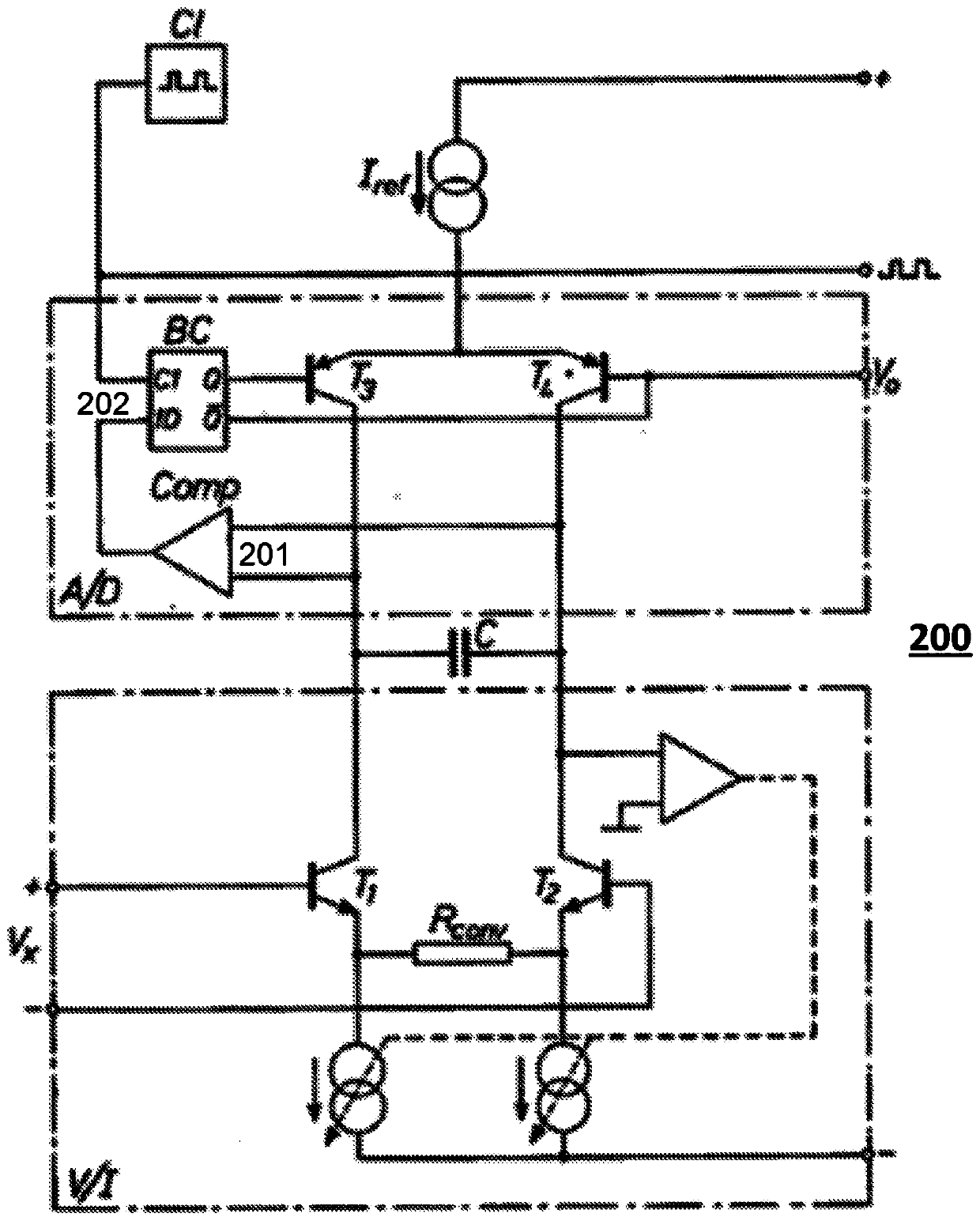
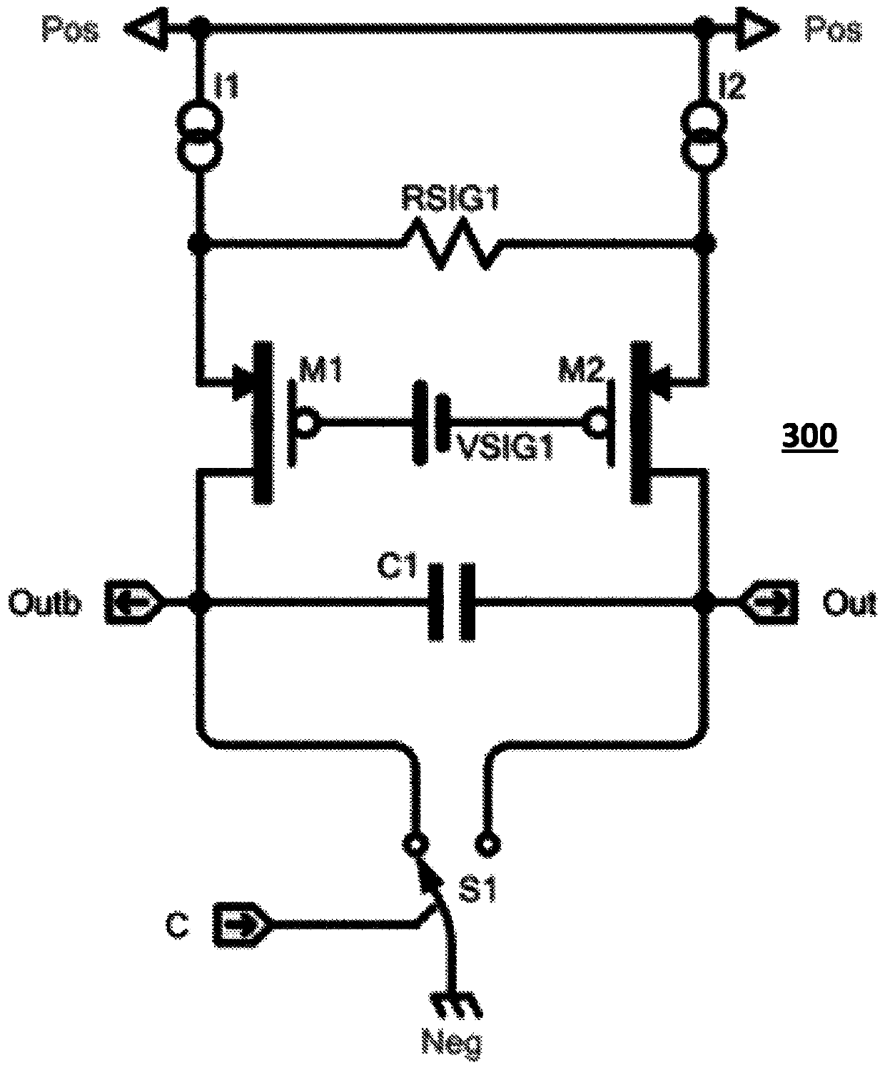
[0018] This application describes an improved ΣΔ modulator that can be used as an ADC. In one embodiment, the ΣΔ modulator has no common mode control loop and no reference current. This results in reduced complexity, ie fewer components, and reduced noise.
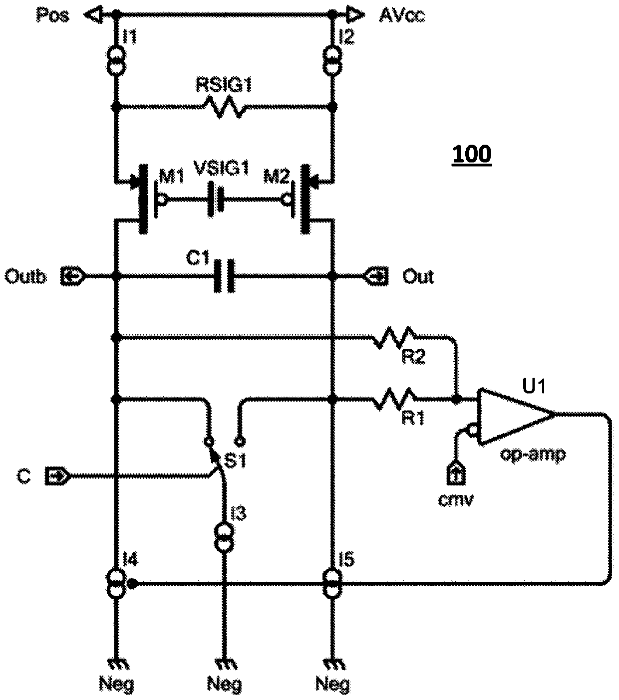
[0019] As mentioned above, figure 1 An example of a prior art ΣΔ modulator circuit 100 is shown in which an input difference current is caused to flow in the drains of transistors M1 and M2. This occurs because a fraction of the nominally equal currents of the current sources I1 and I2 flow through the resistor RSIG1 due to the input voltage VSIG1 which is applied to the gates of the transistors M1 and M2.
[0020] This configuration of the upper part of circuit 100 with current sources I1 and I2, transistors M1 and M2, resistor RSIG1 and input voltage source VSIG1 is well known to those skilled in the art and constitutes what is commonly referred to as voltage-to-current ( V to I) converter. The V to I converter conve...
PUM
 Abstract
Description
Claims
Application Information
 - R&D
- Intellectual Property
- Life Sciences
- Materials
- Tech Scout
- Unparalleled Data Quality
- Higher Quality Content
- 60% Fewer Hallucinations
Browse by: Latest US Patents, China's latest patents, Technical Efficacy Thesaurus, Application Domain, Technology Topic, Popular Technical Reports.
© 2025 PatSnap. All rights reserved.Legal|Privacy policy|Modern Slavery Act Transparency Statement|Sitemap|About US| Contact US: help@patsnap.com


