High-power-density COB device

A high power density, device technology, applied in the direction of electric solid state devices, semiconductor devices, electrical components, etc., can solve the problems of not meeting the market demand, small installation area, etc., achieve small installation area, improve power density, and ensure light output efficiency Effect

Inactive Publication Date: 2020-01-03
FOSHAN EVERCORE OPTOELECTRONICS TECH
View PDF0 Cites 0 Cited by
  • Summary
  • Abstract
  • Description
  • Claims
  • Application Information

AI Technical Summary

Problems solved by technology

With the wide application of COB lighting products, for some COB products with small installation area and high light brightness requirements, the existing practice is to arrange LED chips as densely as possible, but it still cannot meet the market demand.

Method used


Image

  • High-power-density COB device
  • High-power-density COB device
  • High-power-density COB device

Examples


Embodiment Construction

[0021] In order to enable those skilled in the art to better understand the technical solutions of the present invention, the present invention will be further described in detail below in conjunction with the accompanying drawings and preferred embodiments.

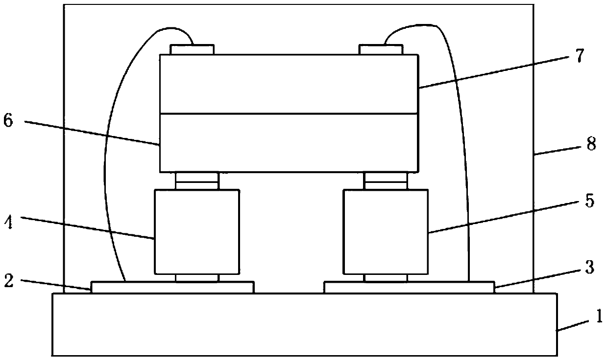
[0022] see figure 1 A high power density COB device provided by the present invention includes a substrate 1 , several laminated structures disposed on the substrate 1 , and an encapsulation layer 8 covering the laminated structures.

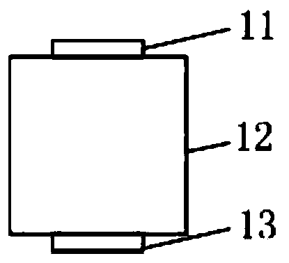
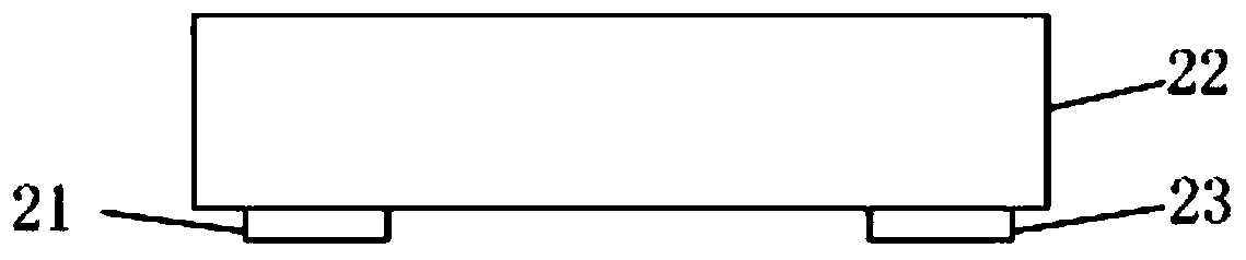
[0023] The laminated structure of the present invention includes a first pad 2 , a second pad 3 , a first vertical chip 4 , a second vertical chip 5 , a flip chip 6 and a front chip 7 .

[0024] The substrate 1 of the present invention is used to install other structures of COB devices, and it can be a ceramic substrate or a metal substrate, and the type of the substrate 1 is selected according to actual needs.

[0025] The first pad 2 and the second pad 3 of the present invention are loc...


PUM


Abstract

The invention relates to a high-power-density COB device. The device comprises a substrate, a plurality of laminated structures arranged on the substrate, and a packaging adhesive layer covering the laminated structures, wherein the laminated structure comprises a first bonding pad, a second bonding pad, a first vertical chip, a second vertical chip, a flip chip and a normal chip, the first bonding pad and the second bonding pad are arranged on the substrate, the first vertical chip is arranged on the first bonding pad, the first vertical chip is arranged on the first bonding pad, the second vertical chip is arranged on the second bonding pad, the flip chip is arranged on the first vertical chip and the second vertical chip so as to form conductive connection between the first vertical chip and the second vertical chip, and the normal chip is arranged on the flip chip and is connected with the first bonding pad and the second bonding pad through wires. The high-power-density COB deviceis advantaged in that a stacked structure is formed, the placement number of LED chips in the same area is increased, so the power density of a COB device is improved.

Description

technical field [0001] The invention relates to the technical field of LED packaging, in particular to a COB device with high power density. Background technique [0002] Ultraviolet and deep ultraviolet LEDs have great application value in medical treatment, sterilization, light curing, 3D printing, printing, lighting, data storage, and secure communication. Due to its small size, simple structure, controllable wavelength, good integration, long life, low energy consumption, and zero pollution, deep ultraviolet LEDs have greater advantages than traditional gas ultraviolet light sources such as mercury lamps and xenon lamps, and have huge social and economic benefits. value. [0003] COB light source packaging, that is, chip-on-board packaging, is one of the bare chip mounting technologies. The LED chip is mounted on the printed circuit board. The electrical connection between the chip and the substrate is realized by wire stitching and covered with resin to ensure reliabil...

Claims


Application Information

Patent Timeline
Patent Type & Authority Applications(China)
IPC IPC(8): H01L25/075H01L33/56H01L33/58
CPCH01L25/0756H01L33/56H01L33/58
Inventor 王孟源曾伟强
Owner FOSHAN EVERCORE OPTOELECTRONICS TECH
Why Eureka
Try Eureka