Array substrate and display device

An array substrate and display area technology, applied in instruments, acquiring/organizing fingerprints/palmprints, optics, etc., can solve the problems of large frame area, high screen ratio limitation, and large size of fingerprint recognition devices, and achieve narrow The effect of borders, increasing screen ratio, and consistent width

Active Publication Date: 2022-07-08
XIAMEN TIANMA MICRO ELECTRONICS
View PDF11 Cites 0 Cited by
  • Summary
  • Abstract
  • Description
  • Claims
  • Application Information

AI Technical Summary

Problems solved by technology

[0003] The display panel in the liquid crystal display generally has a display area and a frame area. The frame area surrounds the display area. Optical devices such as fingerprint identification devices can be arranged in the frame area. Due to the large volume of the fingerprint identification device, the occupied frame area Larger area, resulting in greater restrictions in achieving high screen-to-body ratio and narrow bezel design

Method used


Image

  • Array substrate and display device
  • Array substrate and display device
  • Array substrate and display device

Examples


Embodiment Construction

[0028] Specific implementations of an array substrate and a display device provided by embodiments of the present invention will be described in detail below with reference to the accompanying drawings. It should be noted that the described embodiments are only a part of the embodiments of the present invention, but not all of the embodiments. Based on the embodiments of the present invention, all other embodiments obtained by those of ordinary skill in the art without creative efforts shall fall within the protection scope of the present invention.

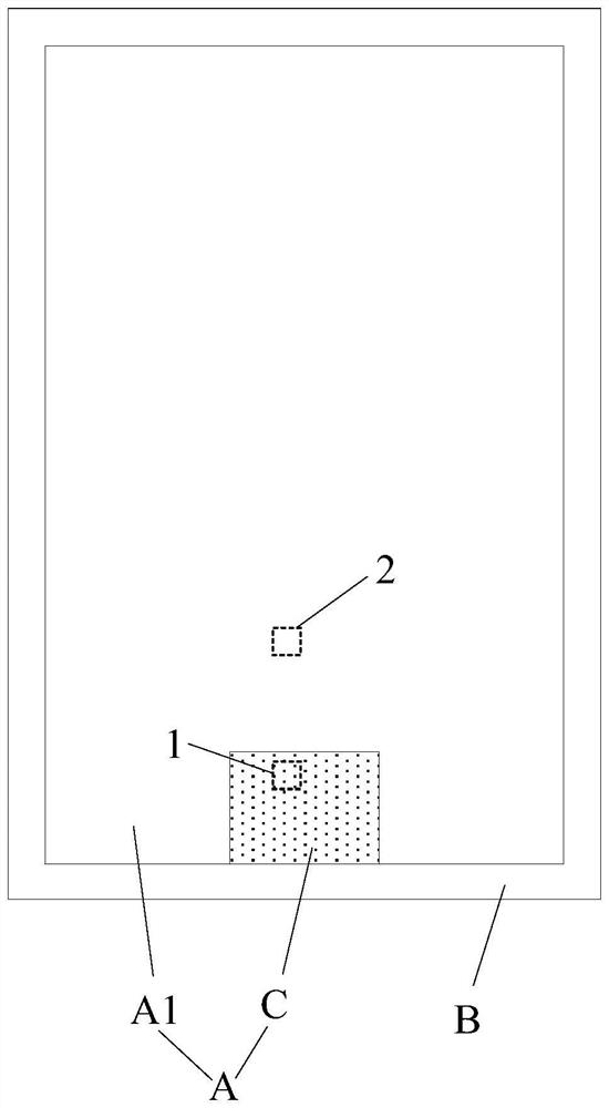
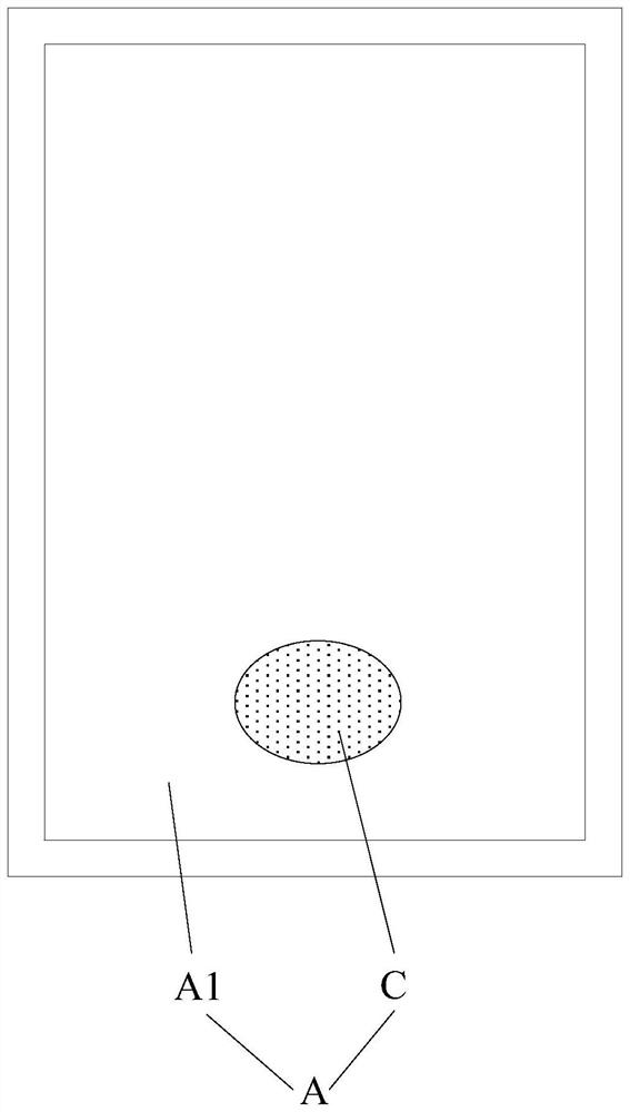
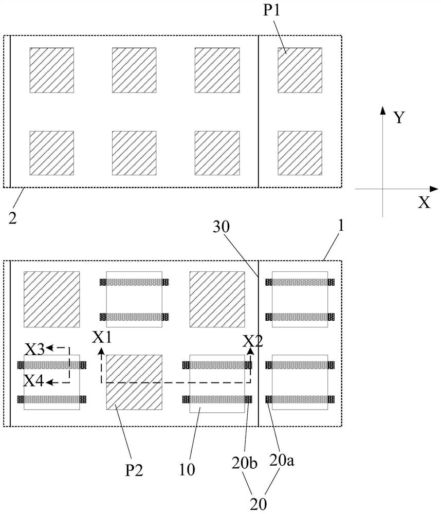
[0029] Embodiments of the present invention provide an array substrate, such as Figure 1 to Figure 6 shown, where, figure 1 is a schematic diagram of the structure of an array substrate, figure 2 is a schematic diagram of the structure of another array substrate, image 3 for figure 1 The partially enlarged schematic diagram in the dashed box 1 and the dashed box 2 in , Figure 4 for along image 3 The cross-sectional vie...


PUM


Abstract

The present invention discloses an array substrate and a display device. In the embodiment of the present invention, the display area includes an optical device setting area. When an optical device is arranged in the optical device setting area, it can avoid that the optical device is arranged on a frame and occupies a relatively large area. This is a big problem, so that the frame can be set narrower, the screen ratio can be increased, and the design of the narrow frame can be realized. Moreover, since the shielding structure includes more than two subsections, the signal lines are correspondingly arranged in the gap between the two adjacent subsections, so that along the extension direction of the signal lines, the area where the signal lines need to be fabricated has a flat surface , to avoid the problem of reducing the exposure accuracy caused by the uneven surface and the step difference, thereby avoiding the problem of disconnection caused by the inconsistent width of the produced signal lines due to low exposure accuracy, and ensuring the obtained signal lines have the same width. , reducing the probability of disconnection, thereby improving the reliability of the array substrate.

Description

technical field [0001] The present invention relates to the field of display technology, in particular to an array substrate and a display device. Background technique [0002] The liquid crystal display is a non-self-luminous device, and a backlight module needs to be set up, and the display function can be realized by using the backlight source provided by the backlight module. [0003] The display panel in a liquid crystal display generally has a display area and a frame area, the frame area surrounds the display area, and optical devices such as fingerprint recognition devices can be arranged in the frame area. Due to the large area, the realization of high screen-to-body ratio and narrow bezel design is greatly restricted. [0004] Then, how to improve the high screen ratio of the display panel and realize the narrow frame design is a technical problem to be solved urgently by those skilled in the art. SUMMARY OF THE INVENTION [0005] Embodiments of the present inv...

Claims


Application Information

Patent Timeline
Patent Type & Authority Patents(China)
IPC IPC(8): G02F1/1362G02F1/1333G06V40/13
CPCG02F1/13338G02F1/136286G02F1/136209G06V40/1324G02F1/13685G02F1/134372G06F3/0421G02F1/133357G06V40/1318
Inventor 杨栩刘博智陈国照
Owner XIAMEN TIANMA MICRO ELECTRONICS
Why Eureka
Try Eureka