Display panel and manufacturing method thereof

A technology for display panels and metal wiring, which is applied in the direction of organic semiconductor devices, electrical components, electric solid devices, etc., can solve problems affecting display, OLED device short circuit, surface pits, etc., to reduce short circuit or abnormal performance, and improve flatness degree of effect

Inactive Publication Date: 2019-12-13
SHENZHEN CHINA STAR OPTOELECTRONICS SEMICON DISPLAY TECH CO LTD
View PDF4 Cites 0 Cited by
  • Summary
  • Abstract
  • Description
  • Claims
  • Application Information

AI Technical Summary

Problems solved by technology

[0005] The present invention provides a display panel and its preparation method to solve the problem of existing display panels. Since a large number of metal wires are used in TFT devices, and the sides of the metal wires generally have burr-like protrusions, which will reflect the exposure of the exposure machine. The planarization layer will absorb the light energy of the reflected light to a certain extent, which affects the local film thickness on the surface of the planarization layer, resulting in burr-like protrusions on the surface of the negative planarization film layer or positive planarization layer. Surface pits, which in turn lead to a short circuit of the OLED device, which in turn affects the technical problems of the display

Method used


Image

  • Display panel and manufacturing method thereof
  • Display panel and manufacturing method thereof
  • Display panel and manufacturing method thereof

Examples


Embodiment Construction

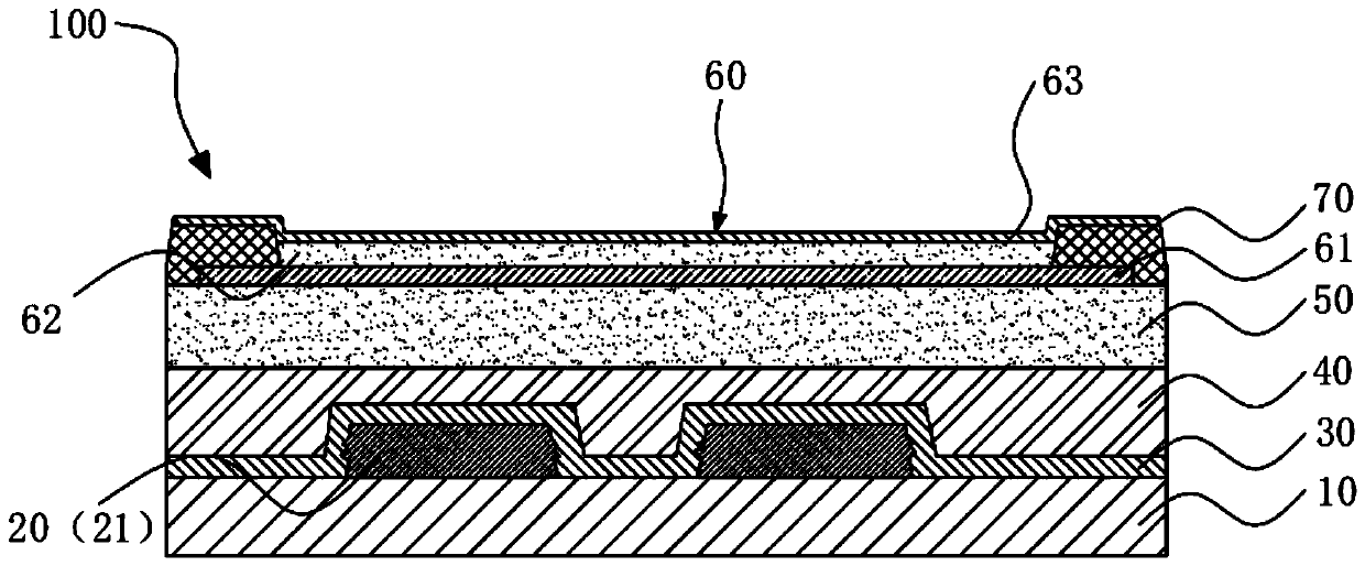
[0026] The following descriptions of the various embodiments refer to the accompanying drawings to illustrate specific embodiments in which the invention may be practiced. The directional terms mentioned in the present invention, such as [top], [bottom], [front], [back], [left], [right], [inside], [outside], [side], etc., are only for reference The orientation of the attached schema. Therefore, the directional terms used are used to illustrate and understand the present invention, but not to limit the present invention. In the figures, structurally similar elements are denoted by the same reference numerals.

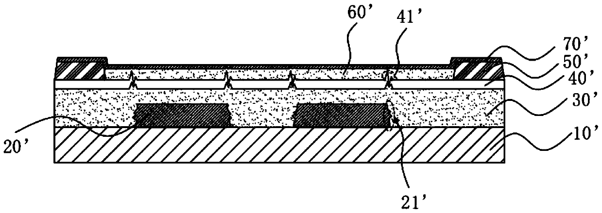
[0027] The present invention is aimed at the existing display panel, because a large amount of metal is used in the TFT device, and the side of the metal wiring has burr-like protrusions, which will reflect the ultraviolet light of the exposure machine, and the planarization layer is an organic photosensitive photoresist. It will absorb the light energy of the reflecte...


PUM


Abstract

The invention discloses a display panel, which comprises a substrate, a metal wiring layer, an OLED light-emitting layer and a barrier layer, wherein the barrier layer is arranged between the metal wiring layer and the OLED light-emitting layer, and the barrier layer covers the metal wiring layer. The barrier layer capable of absorbing ultraviolet light is arranged on the metal wiring layer, ultraviolet light of an exposure machine can be prevented from irradiating the lower metal wiring layer, and thus, when a planarization layer is manufactured subsequently, light of the bottom layer is prevented from being reflected to the planarization layer, the planarization layer is prevented from locally receiving light energy abnormally to generate protrusions or pits, the flatness of a pixel definition area is improved, and the risk of OLED device short circuit or performance abnormity caused by unevenness of a film layer in a pixel is reduced to a great extent.

Description

technical field [0001] The invention relates to the field of display technology, in particular to a display panel and a preparation method thereof. Background technique [0002] With the development of OLED (Organic Light-Emitting Diode, Organic Light-Emitting Diode) technology, there are two ways to prepare OLED devices: evaporation and printing. The thickness of the OLED device between the cathode and the anode is small, usually between 100 ~500 nanometers, so the flatness of the substrate for preparing the OLED device is particularly important, and too large or too steep a step difference in the pixel definition area will cause a short circuit or abnormal performance of the OLED device. [0003] In order to fill the level difference within the pixel definition, a planarization layer is usually made after the TFT (Thin Film Transistor, thin film transistor) device is prepared. The material of the planarization layer is generally an organic photosensitive photoresist, but t...

Claims


Application Information

Patent Timeline
Patent Type & Authority Applications(China)
IPC IPC(8): H01L27/32
CPCH10K59/123H10K59/122H10K59/1315H10K59/1201H10K59/124H10K59/126H10K59/131H10K2102/341H10K71/00
Inventor 何昆鹏唐甲
Owner SHENZHEN CHINA STAR OPTOELECTRONICS SEMICON DISPLAY TECH CO LTD
Why Eureka
Try Eureka