Light emitting device
A technology of light-emitting devices and light-emitting elements, which can be used in projection devices, signal devices, lighting devices, etc., and can solve the problems of inability to distinguish between reflected light and non-reflected light
- Summary
- Abstract
- Description
- Claims
- Application Information
AI Technical Summary
Problems solved by technology
Method used
Image
Examples
no. 1 approach >
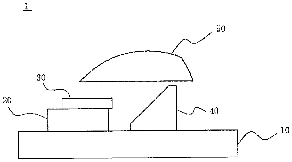
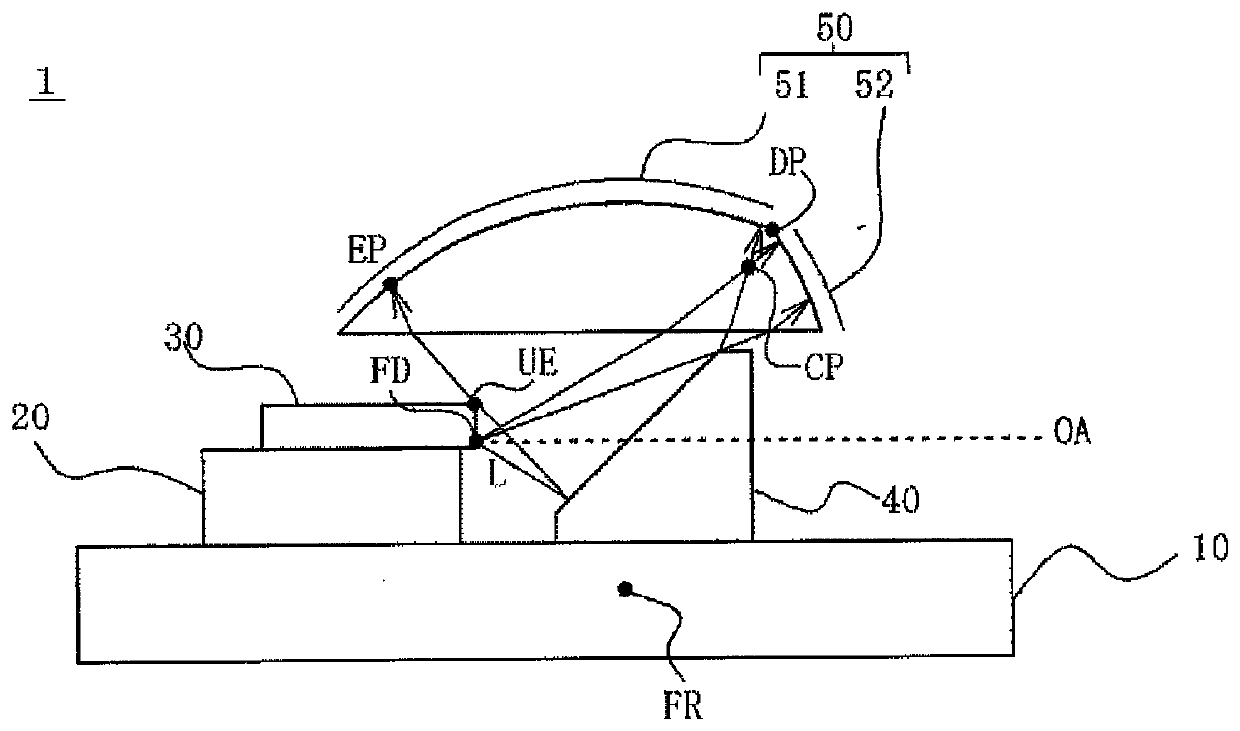
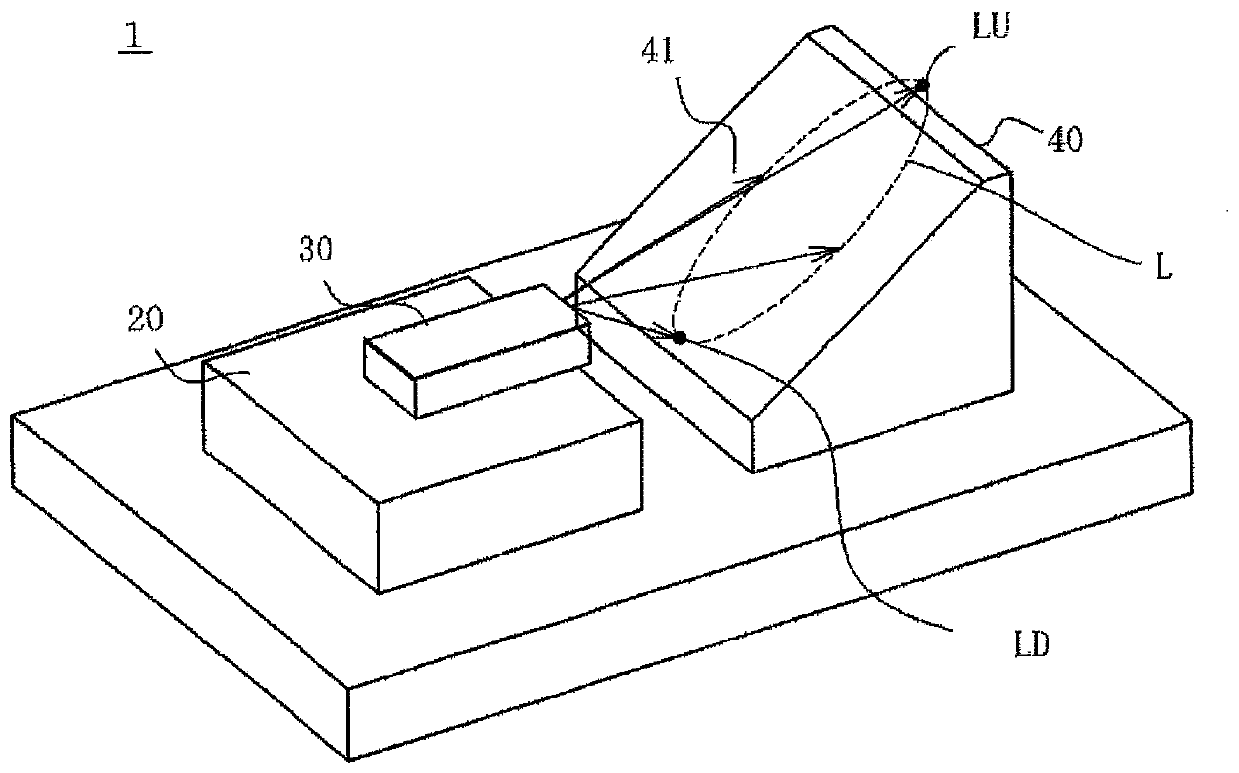
[0022] figure 1 It is a schematic diagram of the light emitting device 1 of the first embodiment. The light-emitting device 1 has a base 10 , a chassis 20 , a semiconductor laser element 30 , a reflective member 40 , and a lens member 50 . In addition, in the light emitting device 1 , the base 20 , the semiconductor laser element 30 , the reflective member 40 , and the lens member 50 are arranged on the plane of the base 10 . In addition, in the light-emitting device 1, the lens member 50 is arranged above the semiconductor laser element 30 and the light reflecting member 40 arranged on the arrangement surface on the base 10 based on the arrangement surface on which the light reflection member 40 is arranged. . Hereinafter, constituent elements of the light emitting device 1 will be described. It should be noted that “above” in this specification refers to the direction in which the semiconductor laser element 30 is arranged based on the arrangement surface of the base 10 ....
no. 2 approach >
[0050] The light emitting device 2 of the second embodiment is a device in which light emitted from a plurality of semiconductor laser elements is emitted to the outside of the light emitting device 2 through a lens member. In addition, the light-emitting device 2 of the second embodiment includes: a package having a light-emitting function for emitting controlled light; and a mounting substrate. It should be noted that there may be no mounting substrate. Figure 5 to Figure 8 It is a figure explaining the light emitting device 2. Figure 5 A perspective view showing a light emitting device 2, Figure 6 It shows a top view of each constituent element disposed in the frame marked with the base 210 of the light emitting device 2, Figure 7 shows a top view of the light emitting device 2, Figure 8 express will Figure 7 The sectional view of the light-emitting device on the straight line connecting VIII-VIII. It should be noted that, for the convenience of explanation, Fi...
Embodiment 1
[0085] Next, an example of the light emitting device 2 shown in the second embodiment will be described. The light-emitting device 2 of Example 1 has a substrate 200 with a side length of about 10 mm, and the side length on the S1 side is longer than the side length on the S2 side by about several mm. In addition, as for the length of the outer surface of the base part 210, the side on the S1 side is about 7.0 mm, and the side on the S2 side is about 6.0 mm. In addition, the height from the lower surface of the bottom of the base 210 to the apex of the lens portion of the lens member 250 is about 5.1 mm, and the light emitting device 2 has a height of about 6.0 mm including the thickness of the substrate 200 .
[0086] The height of the base 210 from the lower surface of the bottom to the upper surface 211 of the side part is about 2.0 mm, the height of the lens part 250 from the lower surface to the apex of the lens part is about 2.5 mm, and the height of the lens part from t...
PUM
 Abstract
Description
Claims
Application Information
 - R&D
- Intellectual Property
- Life Sciences
- Materials
- Tech Scout
- Unparalleled Data Quality
- Higher Quality Content
- 60% Fewer Hallucinations
Browse by: Latest US Patents, China's latest patents, Technical Efficacy Thesaurus, Application Domain, Technology Topic, Popular Technical Reports.
© 2025 PatSnap. All rights reserved.Legal|Privacy policy|Modern Slavery Act Transparency Statement|Sitemap|About US| Contact US: help@patsnap.com


