A kind of equipment for preparing large-area antimony selenide thin film and its method and application
An antimony selenide, large-area technology, applied in the direction of final product manufacturing, sustainable manufacturing/processing, climate sustainability, etc., can solve problems such as inability to prepare large areas and unsatisfactory quality of antimony selenide thin films
- Summary
- Abstract
- Description
- Claims
- Application Information
AI Technical Summary
Problems solved by technology
Method used
Image
Examples
Embodiment 1
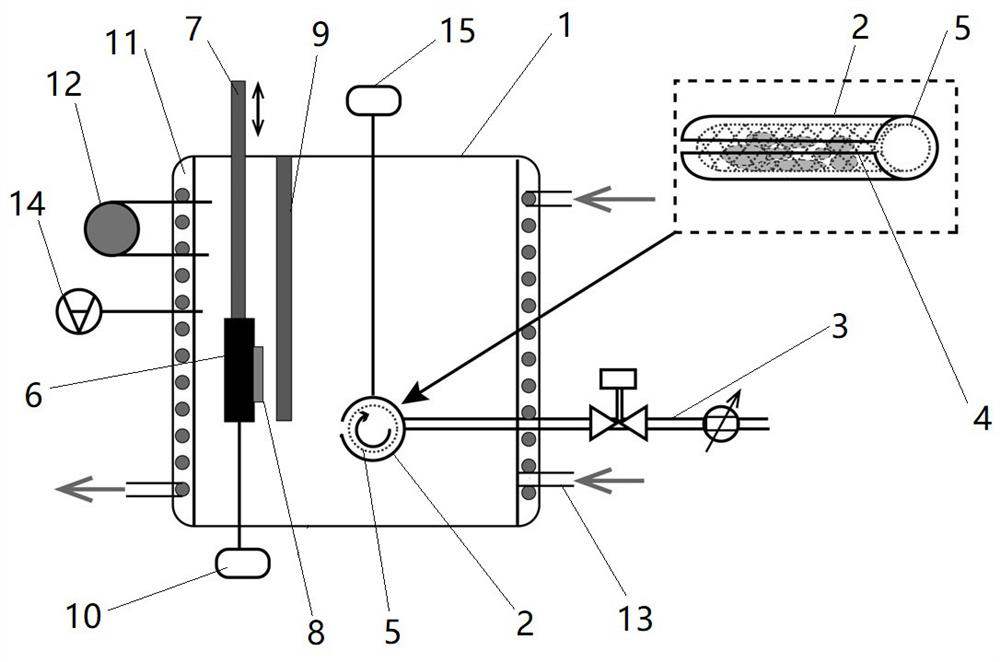
[0028] Such as figure 1 As shown, the equipment of the present invention can be modified on the basis of existing VTD equipment, and its structure is that a cylinder 2 is horizontally fixed in the deposition chamber 1 of the deposition equipment, and one side of the cylinder 2 is connected with the argon gas supply pipe 3 The other side of the cylinder 2 is provided with a horizontally extending elongated hole 4, the other parts of the cylinder 2 are sealed, and a cylindrical hole for containing high-purity antimony selenide particles is coaxially provided in the cylinder 2. Mesh drain 5, the mesh of which is smaller than antimony selenide particles, one end of the mesh drain 5 is connected with a rotating shaft, and the rotating shaft passes through the bearing assembly provided on the end face of the cylinder and is connected to the driving device. The mesh drain 5 can play a role in the driving device. Rotate at a constant speed in cylinder 2.
[0029] A sample stage 6 is ...
Embodiment 2
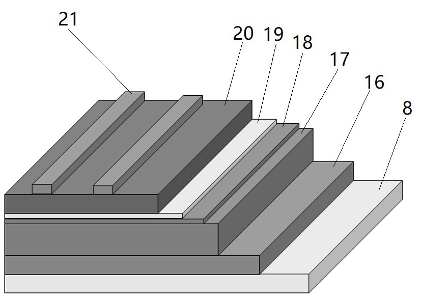
[0033] Apply the present invention to prepare large-area antimony selenide solar cell, the structure of solar cell is glass substrate, molybdenum electrode, antimony selenide film, cadmium sulfide, zinc oxide, aluminum-doped zinc oxide, silver electrode (such as image 3 shown).
[0034] Its preparation process is as follows:
[0035] (1) Preparation of the substrate
[0036] Using glass as a substrate, first soak the glass in an electronic cleaner solution for 12 hours, then take it out, rinse it with deionized water, and finally blow it dry with nitrogen.
[0037] (2) Deposit molybdenum back electrode
[0038] The Mo back electrode was prepared by magnetron sputtering technology, Ar gas was used as the reaction gas, the sputtering pressure was 0.4 Pa, and the sputtering power density was about 4 W / cm 2 , the thickness of the prepared film is about 700 nm, and the resistivity of the prepared film is about 3×10 -5 Ω·cm.
[0039] (3) Deposition of antimony selenide layer ...
PUM
| Property | Measurement | Unit |
|---|---|---|
| electrical resistivity | aaaaa | aaaaa |
Abstract
Description
Claims
Application Information
 - R&D Engineer
- R&D Manager
- IP Professional
- Industry Leading Data Capabilities
- Powerful AI technology
- Patent DNA Extraction
Browse by: Latest US Patents, China's latest patents, Technical Efficacy Thesaurus, Application Domain, Technology Topic, Popular Technical Reports.
© 2024 PatSnap. All rights reserved.Legal|Privacy policy|Modern Slavery Act Transparency Statement|Sitemap|About US| Contact US: help@patsnap.com


