Image stitching method and electronic device using same
A technology for electronic devices and images, applied in television, electrical components, image communication, etc., can solve problems such as multiple computing resources and time
- Summary
- Abstract
- Description
- Claims
- Application Information
AI Technical Summary
Problems solved by technology
Method used
Image
Examples
Embodiment Construction
[0024] Below in conjunction with accompanying drawing, structural principle and working principle of the present invention are specifically described:
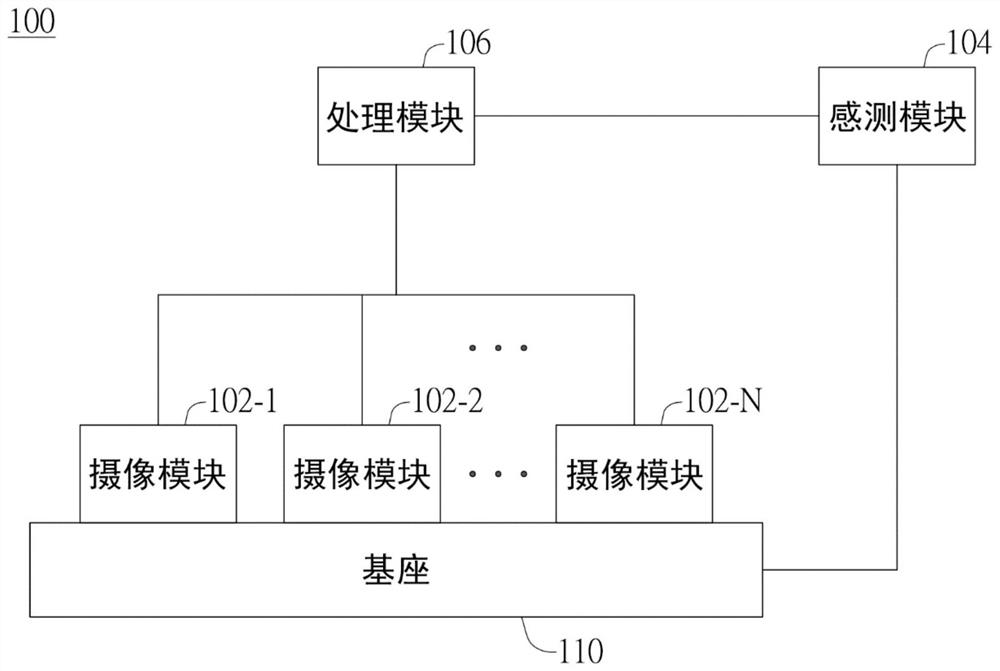
[0025] figure 1 A block diagram of an electronic device 100 according to an embodiment of the invention is shown.
[0026] Please refer to figure 1 , the electronic device 100 includes a bendable base 110 , a plurality of camera modules 102 - 1 - 102 -N (N is a positive integer greater than 1), a sensing module 104 and a processing module 106 . The base 110 may have a bendable mechanism (such as a pivot), and / or be made of any foldable material such as plastic or resin. The camera modules 102 - 1 - 102 -N may be Charge-Coupled Device (CCD) sensors, Complementary Metal-Oxide-Semiconductor (CMOS) sensors or other camera devices. The sensing module 104 can be an accelerometer, a gyroscope, a distance sensor, a resistance / capacitance sensing element, or any sensor capable of detecting changes in the bending angle of the base 11...
PUM
 Abstract
Description
Claims
Application Information
 - R&D
- Intellectual Property
- Life Sciences
- Materials
- Tech Scout
- Unparalleled Data Quality
- Higher Quality Content
- 60% Fewer Hallucinations
Browse by: Latest US Patents, China's latest patents, Technical Efficacy Thesaurus, Application Domain, Technology Topic, Popular Technical Reports.
© 2025 PatSnap. All rights reserved.Legal|Privacy policy|Modern Slavery Act Transparency Statement|Sitemap|About US| Contact US: help@patsnap.com


