
Patsnap Eureka
For R&D, Patsnap Eureka makes reading and utilizing patents & technical documents easy.
Patsnap Eureka AIR
Designed for self-driven R&D workflows. Generate viable solutions, solve complex R&D challenges, empower your innovation with AI.

Patsnap Eureka Materials
Designed for material experts only. Revolutionize your material R&D, from search, analyze, to developing new materials.

TechResearch
Generate reliable direction feasibility study reports for your R&D in just a few steps.

TechSeek
Discover and master advanced knowledge NOW. Basics, ideas, possibilities, all at once.

TechMind
As an expert in R&D Theories, TechMind can generates customized viable solutions instantly.

TechRisk
Analyze your overall solution with one click, know your potential R&D risks in advance.

TechMonitor
Get weekly tech updates, stay abreast of the latest tech innovations and key insights.
Avalanche photodiode and manufacturing method thereof
An avalanche photoelectric and diode technology, which is applied in the direction of circuits, electrical components, semiconductor devices, etc., can solve the problem that the edge area of zinc expansion is difficult to control, and achieve the effect of solving the difficulty of production
- Summary
- Abstract
- Description
- Claims
- Application Information
AI Technical Summary
Problems solved by technology
Method used
Image

Examples
Embodiment Construction
[0040] The present invention will be described in further detail below in conjunction with the accompanying drawings and embodiments.
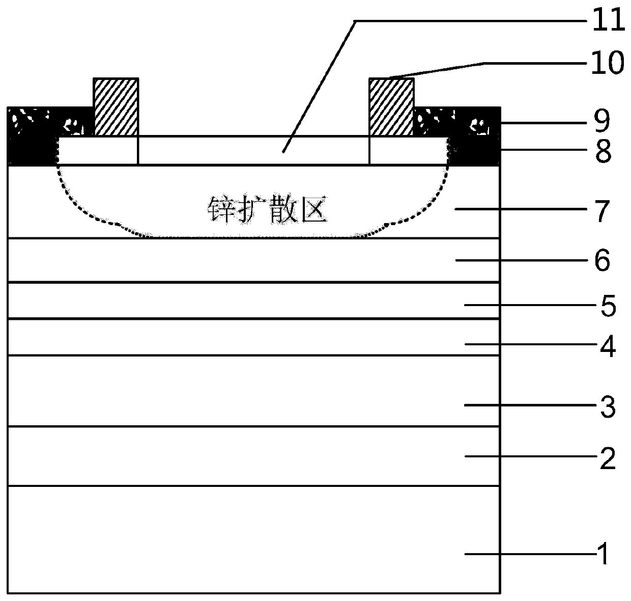
[0041] figure 1 It is a schematic structural diagram of an avalanche photodiode in an embodiment of the present invention, as figure 1 As shown, on the one hand, an embodiment of the present invention provides an avalanche photodiode, and the avalanche photodiode includes:
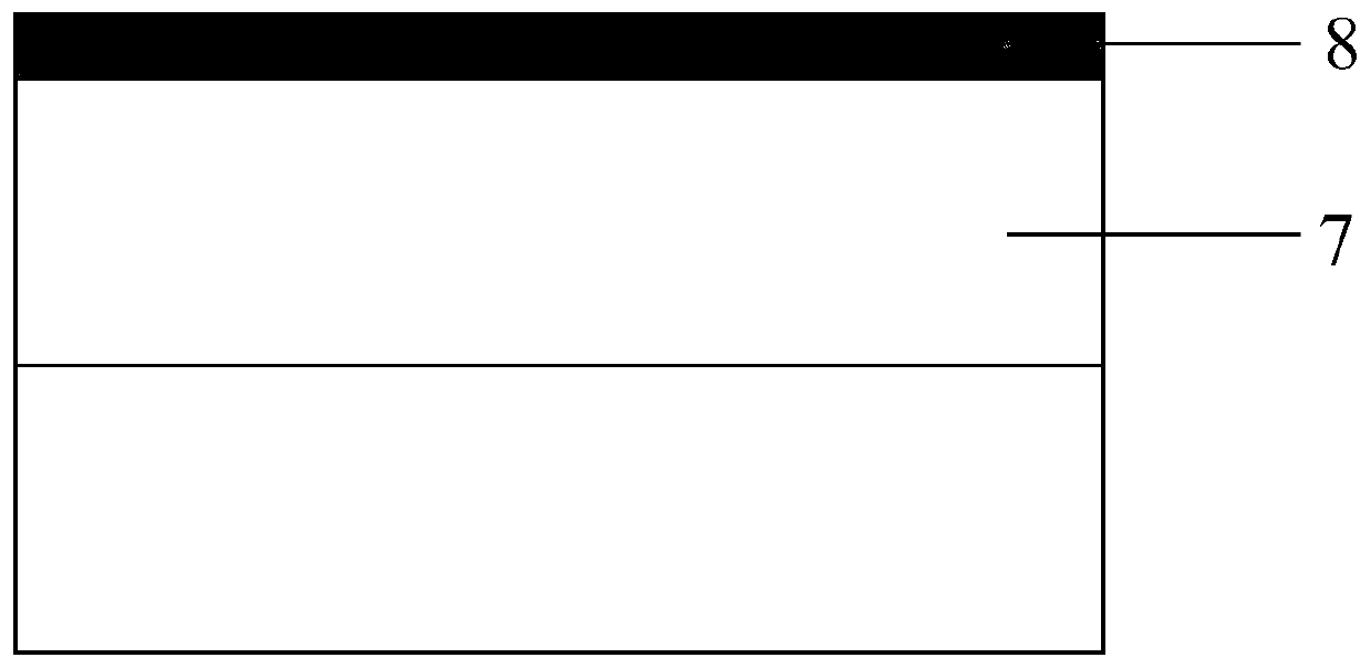
[0042] A substrate 1 on which a first contact layer 7 is provided;
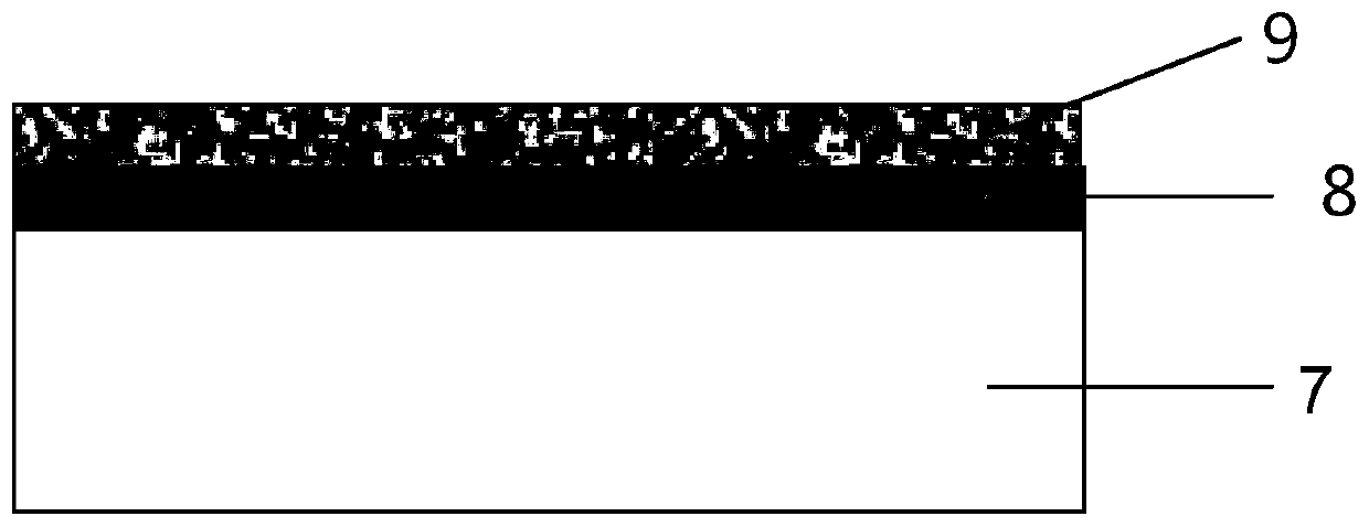
[0043] The second contact layer 8, which is plated on the first contact layer 7, and the second contact layer 8 is provided with a first window 81;
[0044] The passivation layer 9, which is plated on the second contact layer 8, and the passivation layer 9 is provided with a second window 91, the cross-sectional area of the second window 91 is larger than the cross-sectional area of the first window 81, and the second window 91 The second window 91 and the first window 81 are stepped; and
[0045]...
PUM
 Abstract
Description
Claims
Application Information
 - R&D Engineer
- R&D Manager
- IP Professional
- Industry Leading Data Capabilities
- Powerful AI technology
- Patent DNA Extraction
Browse by: Latest US Patents, China's latest patents, Technical Efficacy Thesaurus, Application Domain, Technology Topic, Popular Technical Reports.
© 2024 PatSnap. All rights reserved.Legal|Privacy policy|Modern Slavery Act Transparency Statement|Sitemap|About US| Contact US: help@patsnap.com