Perovskite film forming process
A perovskite and film-forming technology, applied in the field of perovskite solar cells, can solve the problems of reducing film-forming quality, film damage, and scratching head hardness, and achieve the effects of avoiding film damage, efficient preparation, and accurate film thickness regulation.
- Summary
- Abstract
- Description
- Claims
- Application Information
AI Technical Summary
Problems solved by technology
Method used
Image
Examples
Embodiment 1
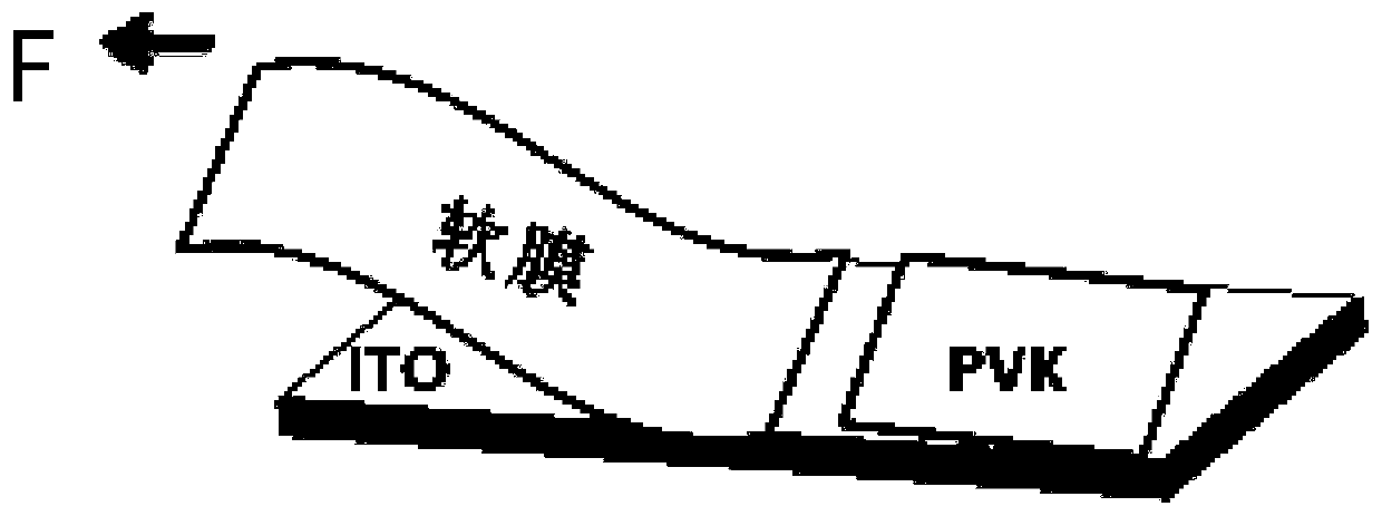
[0020] Example 1 A polyimide film (PI) with an area of 1cm*1cm is softly covered with a brush film, the substrate area is 1cm*10cm, and a volume of 50 μL of perovskite precursor solution is dripped on the leftmost edge of the substrate , the precursor component is PbI 2 The molar ratio of MAI and MAI is 1.07:1, and the PI film is brushed at a slow and uniform speed, and the speed of brushing the film is adjusted to be 2mm / s constant, so that the precursor solution can be uniformly covered on the substrate. quality perovskite films.
Embodiment 2
[0021] Embodiment 2 uses the soft film with hydrophobic precursor liquid performance to be used for soft covering brush film, and area is 5cm*5cm, and substrate area is 10cm*10cm, and precursor liquid component is PbI 2 The molar ratio of MAI and MAI is 1.07:1, drop 100 μL of precursor solution on the substrate, and brush the film at a speed of 0.5mm / s-2mm / s to brush the film at a variable speed. The obtained precursor solution can evenly cover the substrate, and anneal at 140°C for 15 minutes A uniform high-quality perovskite film is obtained.
Embodiment 3
[0022] Example 3 The hydrophobic soft film and the hydrophilic soft film are respectively used in the same precursor solution, and the precursor solution component is PbI 2 With a molar ratio of 1.07:1 to MAI, take the same volume of 20 μL and drop it on a 1mm*1mm substrate. The brushing rate is 2mm / s, and the annealing time is 10min. Perovskite crystals with different crystal sizes and film properties are prepared. film.
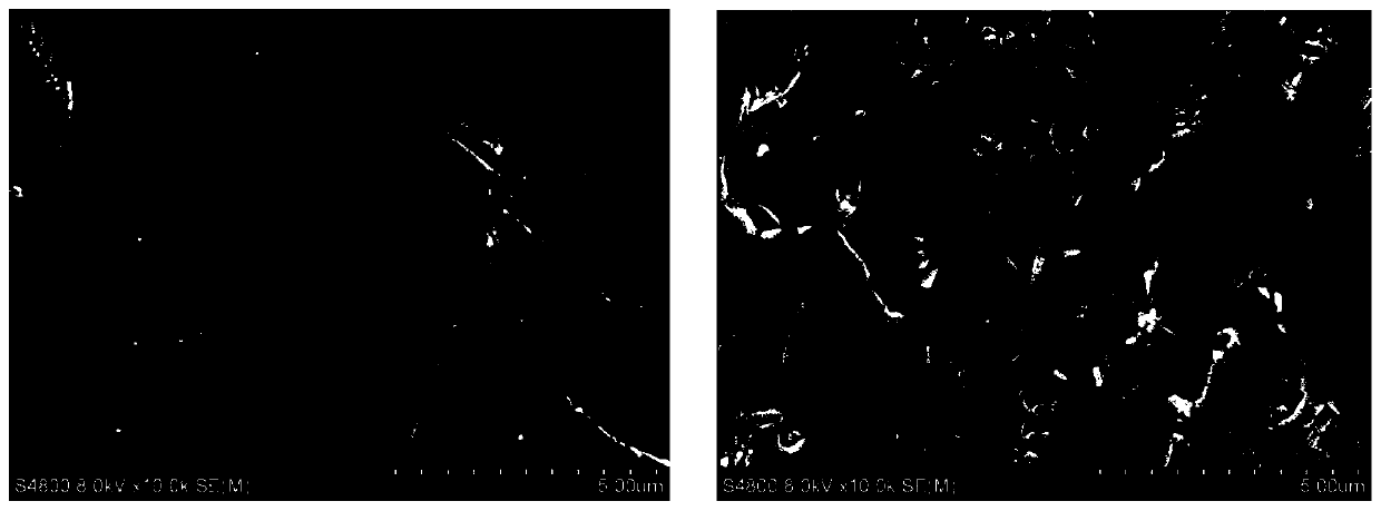
[0023] soft cover film Surface Roughness of Perovskite Films Cracks on the surface of the perovskite film Parafilm Small less PI film larger more
[0024] Specific comparison such as figure 2 shown. figure 2 The picture on the left shows the annealed perovskite surface brushed out by the PI film at a size of 5 μm, with large roughness and many cracks. figure 2 The picture on the right shows the annealed perovskite surface brushed out by the parafilm at a size of 5 μm, with small roughness and fewer cracks.
PUM
| Property | Measurement | Unit |
|---|---|---|
| Thickness | aaaaa | aaaaa |
Abstract
Description
Claims
Application Information
 - R&D
- Intellectual Property
- Life Sciences
- Materials
- Tech Scout
- Unparalleled Data Quality
- Higher Quality Content
- 60% Fewer Hallucinations
Browse by: Latest US Patents, China's latest patents, Technical Efficacy Thesaurus, Application Domain, Technology Topic, Popular Technical Reports.
© 2025 PatSnap. All rights reserved.Legal|Privacy policy|Modern Slavery Act Transparency Statement|Sitemap|About US| Contact US: help@patsnap.com


