
Laminated structure for three-dimensional memory, three-dimensional memory and preparation method thereof

A technology of stack structure and memory, applied in semiconductor devices, electric solid state devices, electrical components, etc., can solve the problems of wide threshold voltage distribution of three-dimensional memory, fast programming/erasing speed, serious memory cell read interference, etc.

Active Publication Date: 2020-10-23
YANGTZE MEMORY TECH CO LTD
View PDF6 Cites 2 Cited by
  • Summary
  • Abstract
  • Description
  • Claims
  • Application Information

AI Technical Summary

Problems solved by technology

[0003] In view of the shortcomings of the prior art described above, the purpose of the present invention is to provide a stacked structure for a three-dimensional memory, a three-dimensional memory and its preparation method. The layer structure, three-dimensional memory and its preparation method are used to solve the problem in the prior art that the memory cells corresponding to the smaller part of the channel via hole width are compared with the memory cells corresponding to the larger part of the channel via hole width. The programming / erasing speed is fast, the memory cells corresponding to the smaller part of the channel via hole have more serious read interference, the erased state coupling effect is poor, and the characteristics of the memory cells in each part of the memory are inconsistent, resulting in the threshold voltage of the three-dimensional memory The distribution is wide, which affects the performance of the three-dimensional memory and other issues

Method used


Image

  • Laminated structure for three-dimensional memory, three-dimensional memory and preparation method thereof
  • Laminated structure for three-dimensional memory, three-dimensional memory and preparation method thereof
  • Laminated structure for three-dimensional memory, three-dimensional memory and preparation method thereof

Examples


Embodiment 1

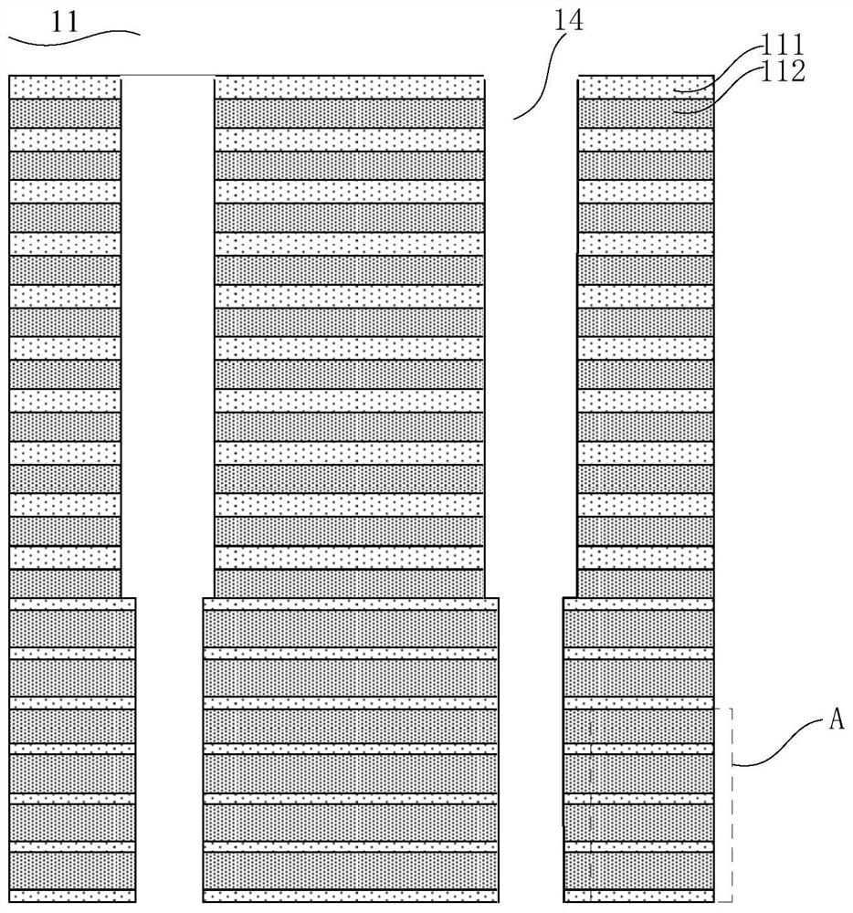
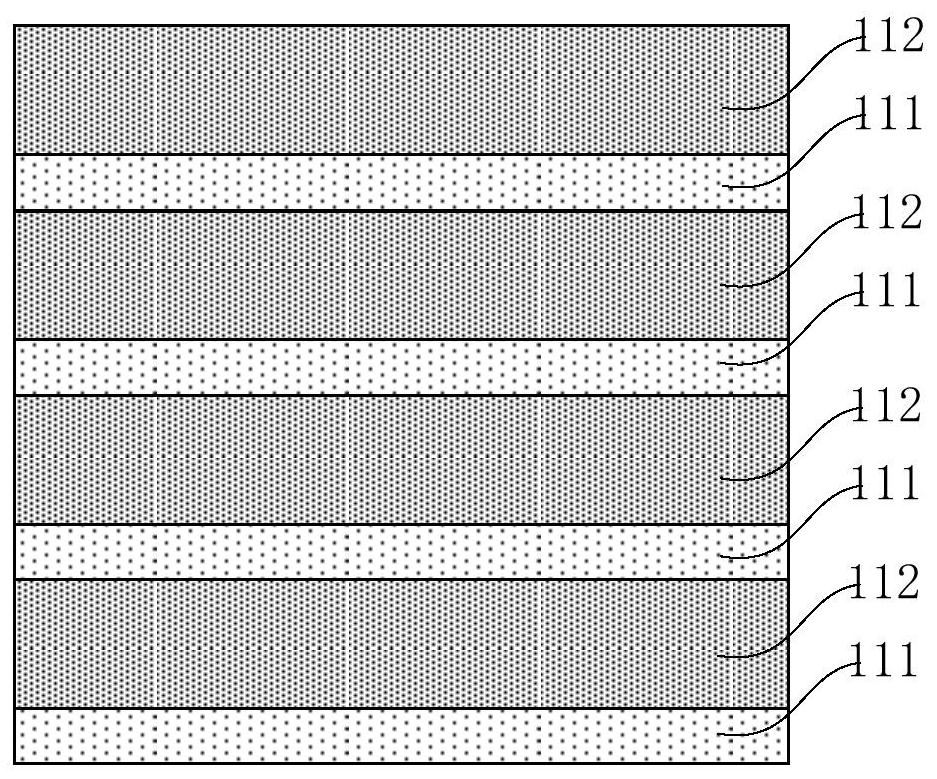
[0115] see figure 1 , the present invention provides a stacked structure 11 for a three-dimensional memory, the stacked structure 11 for a three-dimensional memory includes sacrificial layers and inter-gate dielectric layers alternately stacked up and down; the stacked structure 11 is formed with Along the thickness direction of the stacked structure 11, the channel via hole 14 passing through the stacked structure 11, along the thickness direction of the stacked structure 11, the width of each part of the channel via hole 14 is not the same; The thickness of the sacrificial layer 111 is directly proportional to the width of the channel via 14 and the thickness of the inter-gate dielectric layer 112 is inversely proportional to the width of the channel via 14 .

[0116] As an example, the laminated structure 11 can be divided into an upper part and a lower part from top to bottom along the thickness direction of the laminated structure 11, and the ratio of the upper part of th...

Embodiment 2

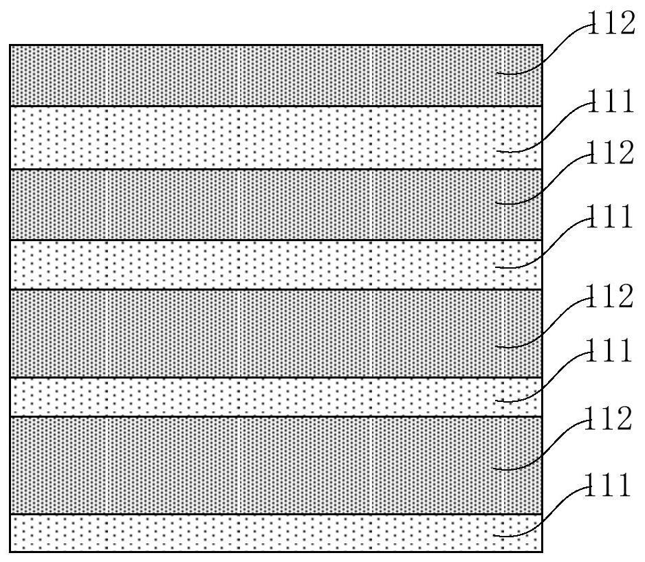
[0138] see Figure 11 The present invention provides a stacked structure 12 for a three-dimensional memory, the stacked structure 12 for a three-dimensional memory includes sacrificial layers and inter-gate dielectric layers alternately stacked up and down; the stacked structure 12 is formed with Along the thickness direction of the stacked structure 12, the channel via hole 14 passing through the stacked structure 12, along the thickness direction of the stacked structure 12, the width of each part of the channel via hole 14 is not the same; The thickness of the gate layer 121 is directly proportional to the width of the channel via 14 and the thickness of the inter-gate dielectric layer 112 is inversely proportional to the width of the channel via 14 .

[0139] As an example, the laminated structure 12 can be divided into an upper part and a lower part from top to bottom along the thickness direction of the laminated structure 12, and the ratio of the upper part of the lamin...

Embodiment 3

[0161] see Figure 21 , the present invention also provides a method for preparing a three-dimensional memory, the method for preparing a three-dimensional memory includes the following steps:

[0162] 1) Provide a semiconductor substrate;

[0163] 2) forming a stacked structure as described in Embodiment 1 on the semiconductor substrate;

[0164] 3) forming an epitaxial layer at the bottom of the channel via hole;

[0165] 4) forming a functional sidewall on the sidewall of the channel via hole, and forming a channel layer on the surface of the functional sidewall and the upper surface of the epitaxial layer;

[0166] 5) forming a gate gap in the stacked structure;

[0167] 6) removing the sacrificial layer based on the gate gap to form a sacrificial gap; and

[0168] 7) Forming a gate layer in the sacrificial gap.

[0169] In step 1), see Figure 21 Step S1 in and Figure 22 , providing a semiconductor substrate 13 .

[0170] As an example, the semiconductor substrat...


PUM


Abstract

The invention provides a stacked structure for a three-dimensional memory, a three-dimensional memory and a preparation method thereof, including sacrificial layers and inter-gate dielectric layers alternately stacked up and down; The channel via hole of the layer structure, along the thickness direction of the laminated structure, the width of each part of the channel via hole is not the same; the thickness of the sacrificial layer is proportional to the width of the channel via hole and the thickness of the inter-gate dielectric layer is proportional Inversely proportional to the width of the via hole. The stacked structure for the three-dimensional memory of the present invention can compensate for the influence of the inconsistency of the width of the channel via hole formed in the stacked structure and the poor shape of the channel via hole; the stacked layer of the three-dimensional memory based on the present invention In the three-dimensional memory formed by the structure, all memory cells have the same programming / erasing speed, the coupling effect of the erased state is better, the performance of all memory cells has better uniformity, the threshold voltage of the three-dimensional memory is narrow, and the performance of the three-dimensional memory Good stability.

Description

technical field [0001] The invention belongs to the technical field of integrated circuit design and manufacture, and in particular relates to a stacked structure for a three-dimensional memory, a three-dimensional memory and a preparation method thereof. Background technique [0002] In the existing semiconductor process, with the continuous improvement of memory density requirements, the number of stacked structures in the three-dimensional memory is continuously increased, and the aspect ratio of the channel vias (CH) formed in the stacked structures is also increasing. Higher and higher. For channel vias with a high aspect ratio, due to the limitation of the existing etching process, the bottom morphology of the formed channel vias is relatively poor, for example, the morphology of the bottom of the channel vias will be deformed (distortion) Or there are defects such as streaks (striation), and at the same time, the width of the channel vias formed is inconsistent, for ...

Claims


Application Information

Patent Timeline
Patent Type & Authority Patents(China)
IPC IPC(8): H01L27/11568H01L27/11582H01L27/115H10B43/30H10B43/10H10B43/27H10B69/00
CPCH10B43/30H10B69/00H10B43/27H10B41/27H10B43/10
Inventor 王启光周文犀
Owner YANGTZE MEMORY TECH CO LTD
Learn More